CA3060
4. Calculation of Bias Resistance. For minimum supply
current drain the amplifier bias current I should be fed
0
-20
-40
-60
-80
ABC
directly from the supplies and not from the bias regulator.
R
C
= 10kΩ
L
L
The value of the resistor R
using Ohm’s law.
may be directly calculated
ABC
= 0
V
– V
ABC
SUP
R
= -------------------------------------
ABC
I
ABC
12 – 0.63
= -------------------------
–6
R
R
ABC
ABC
20 × 10
R
C
= 10kΩ
L
L
= 15pF
= 568.5kΩ or 560kΩ
0.01
0.1
1.0
10
100
5. Calculation of Offset Adjustment Circuit. In order to
reduce the loading effect of the offset adjustment circuit
on the power supply, the offset control should be
arranged to provide the necessary offset current. The
source resistance of the non-inverting input is made
equal to the source resistance of the inverting input,
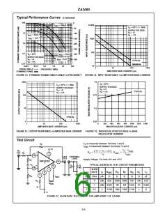
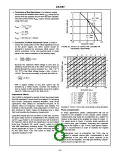
FREQUENCY (MHz)
FIGURE 20. EFFECT OF CAPACITIVE LOADING ON
FREQUENCY RESPONSE
A
B
C
D
E
F
G
1000
100
10
20kΩ × 200kΩ
20kΩ + 200kΩ
---------------------------------------
i.e.,
18kΩ
H
I
Because the maximum offset voltage is 5mV plus an
additional increment due to the offset current (Figure 2)
J
K
L
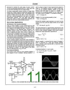
-9
flowing through the source resistance (i.e., 200 x 10
x
3
18 x 10 V), the Offset Voltage Range = 5mV + 3.6mV =
±8.6mV. The current necessary to provide this offset is:
8.6mV
18kΩ
-----------------
0.48µA
1
With a supply voltage of ±6V, this current can be
provided by a 10MΩ resistor. However, the stability of
such a resistor is often questionable and a more realistic
value of 2.2MΩ was used in the final circuit.
0.01
0.1
1.0
10
100
SLEW RATE (V/µs)
A. C = 10,000pF
B. C = 3,000pF
G. C = 10pF
L
H. C = 3pF
L
Capacitance Effects
L
L
C. C = 1000pF
L
I.
C = 1pF
L
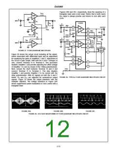
The CA3060 is designed to operate at such low power levels
that high impedance circuits must be employed. In designing
such circuits, particularly feedback amplifiers, stray circuit
capacitance must always be considered because of its
adverse effect on frequency response and stability. For
example a 10kΩ load with a stray capacitance of 15pF has a
time constant of 1MHz. Figure 20 illustrates how a 10kΩ
15pF load modifies the frequency characteristic.
D. C = 300pF
J. C = 0.3pF
K. C = 0.1pF
L. C = 0.03pF
L
L
L
E. C = 100pF
L
L
F. C = 30pF
L
FIGURE 21. EFFECT OF LOAD CAPACITANCE ON SLEW RATE
Phase Compensation
In many applications phase compensation will not be
required for the amplifiers of the CA3060. When needed,
compensation may easily be accomplished by a simple RC
network at the input of the amplifier as shown in Figure 17.
The values given in Figure 17 provide stable operation for
the critical unity gain condition, assuming that capacitive
loading on the output is 13pF or less. Input phase compen-
sation is recommended in order to maintain the highest
possible slew rate.
Capacitive loading also has an effect on slew rate; because
the peak output current is established by the amplifier bias
current, I
(Figure 5), the maximum slew rate is limited to
ABC
the maximum rate at which the capacitance can be charged
by the I . Therefore, SR = dv/dt = I /C , where C is the
OM OM
L
L
total load capacitance including strays. This relationship is
shown graphically in Figure 21. When measuring slew rate
for this data sheet, care was taken to keep the total
capacitive loading to 13pF.
In applications such as integrators, two OTAs may be
cascaded to improve current gain. Compensation is best
accomplished in this case with a shunt capacitor at the
output of the first amplifier. The high gain following compen-
sation assures a high slew rate.
3-8

 HARRIS [ HARRIS CORPORATION ]