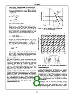
CA3060
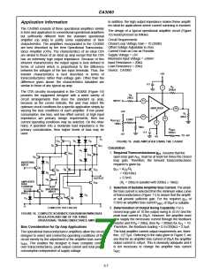
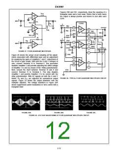
Figures 29B and 29C, respectively, show the squaring of a
I
-
O(1)
triangular wave and a sine wave. Notice that in both cases
the output is always positive and returns to zero after each
cycle.
AMP
1
+
X
V
INPUT
O
R
R
1
2
I
I
ABC (1)
+
CA3060
R
L
X
INPUT
1MΩ
1MΩ
13
OUTPUT
AMP
-
AMP
1
2
16
15
14
I
O(2)
270Ω
1MΩ
1MΩ
100Ω
ABC (2)
270Ω
51kΩ
R
F
200kΩ
270Ω
Y
4
INPUT
R
IN
51
kΩ
-
Y
4
5
INPUT
AMP
3
AMP
3
560kΩ
7
6
100Ω
+
240kΩ
0.02µF
V+
V-
100kΩ
100kΩ
24kΩ
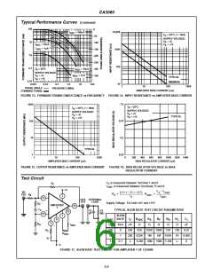
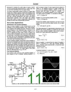
FIGURE 27. FOUR QUADRANT MULTIPLIER
3
1.1MΩ
Figure 28 shows the actual circuit including all the adjust-
ments associated with differential input and an adjustment
for equalizing the gains of Amplifiers 1 and 2. Adjustment of
the circuit is quite simple. With both the X and Y voltages at
zero, connect Terminal 10 to Terminal 8. This procedure
disables Amplifier 2 and permits adjusting the offset voltage
of Amplifier 1 to zero by means of the 100kΩ potentiometer.
Next, remove the short between Terminal 10 and 8 and
connect Terminal 15 to Terminal 8. This step disables
Amplifier 1 and permits Amplifier 2 to be zeroed with the
other potentiometer. With AC signals on both the X and Y
10
11
12
AMP
2
9
8
560kΩ
270Ω
FIGURE 28. TYPICAL FOUR QUADRANT MULTIPLIER CIRCUIT
inputs, R and R
are adjusted for symmetrical output
3
11
signals. Figure 29 shows the output waveform with the
multiplier adjusted. The voltage waveform in Figure 29A
shows suppressed carrier modulation of 1kHz carrier with a
triangular wave.
FIGURE 29A.
FIGURE 29B.
FIGURE 29C.
FIGURE 29. VOLTAGE WAVEFORMS OF FOUR QUADRANT MULTIPLIER CIRCUIT
3-12

 HARRIS [ HARRIS CORPORATION ]