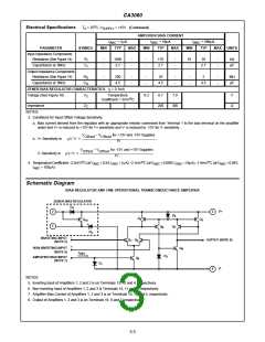
CA3060
In addition, the high output impedance makes these amplifi-
ers ideal for applications where current summing is involved.
Application Information
The CA3060 consists of three operational amplifiers similar
in form and application to conventional operational amplifiers
but sufficiently different from the standard operational
amplifier (op amp) to justify some explanation of their
characteristics. The amplifiers incorporated in the CA3060
are best described by the term Operational Transconduc-
tance Amplifier (OTA). The characteristics of an ideal OTA
are similar to those of an ideal op amp except that the OTA
has an extremely high output impedance. Because of this
inherent characteristics the output signal is best defined in
terms of current which is proportional to the difference
between the voltages of the two input terminals. Thus, the
transfer characteristics is best described in terms of
transconductance rather than voltage gain. Other than the
difference given above, the characteristics tabulated are
similar to those of any typical op amp.
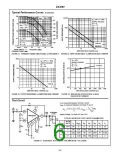
The design of a typical operational amplifier circuit (Figure
19) would proceed as follows:
Circuit Requirements
Closed Loop Voltage Gain = 10 (20dB)
Offset Voltage Adjustable to Zero
Current Drain as Low as Possible
Supply Voltage = ±6V
Maximum Input Voltage = ±50mV
Input Resistance = 20kΩ
Load Resistance = 20kΩ
Device: CA3060
+6V
0.1
R
3
F
200kΩ
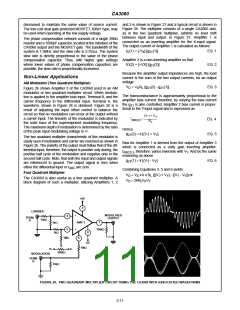
The OTA circuitry incorporated in the CA3060 (Figure 18)
provides the equipment designer with a wider variety of
circuit arrangements than does the standard op amp;
because as the curves indicate, the user may select the
optimum circuit conditions for a specific application simply by
varying the bias conditions of each amplifier. If low power
consumption, low bias, and low offset current, or high input
impedance are primary design requirements, then low
current operating conditions may be selected. On the other
hand, if operation into a moderate load impedance is the
primary consideration, then higher levels of bias may be
used.
R
20kΩ
S
13
INPUT
-
AMPLIFIER
1
16
+6V
R
20kΩ
L
+
14
15
2.2MΩ
R
OFFSET
<4MΩ
8
18kΩ
R
ABC
560kΩ
0.1
-6V
TO +6V
-6V
V+
Q
D
D
6
11
5
FIGURE 19. 20dB AMPLIFIER USING THE CA3060
Q
Q
7
15
Calculation
D
D
7
1. Required Transconductance g . Assume that the
Q
10
21
Q
14
open loop gain A must be at least ten times the closed
loop gain. Therefore, the forward transconductance
required is given by:
Q
3
OL
8
D
INVERTING
INPUT
2
Q
2
g
= A /R
OL
Q
Q
13
-
21
L
Q
9
5
D
Q
3
= 100/18kΩ
+
5.5mS
OUTPUT
4
AMPLIFIER
BIAS
Q
(R = 20kΩ in parallel with 200kΩ 18kΩ)
12
L
CURRENT
NON-
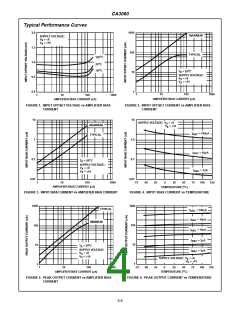
2. Selection of Suitable Amplifier Bias Current. The ampli-
fier bias current is selected from the minimum value curve
of transconductance (Figure 11) to assure that the amplifi-
INVERTING
INPUT
Q
1
(ABC)
D
4
Q
Q
8
D
1
6
er will provide sufficient gain. For the required g
5.5mS an amplifier bias current I
ABC
of
of 20µA is suitable.
21
V-
V-
COMPLETE OTA CIRCUIT
3. Determination of Output Swing Capability. For a
closed loop gain of 10 the output swing is ±0.5V and the
peak load current is 25µA. However, the amplifier must
also supply the necessary current through the feedback
FIGURE 18. COMPLETE SCHEMATIC DIAGRAM SHOWING BIAS
REGULATOR AND ONE OF THE THREE
OPERATIONAL TRANSCONDUCTANCE AMPLIFIERS
resistor and if R = 20kΩ, then R = 200kΩ for A = 10.
S
F
CL
Bias Consideration for Op Amp Applications
Therefore, the feedback loading = 0.5V/200kΩ = 2.5µA.
The total amplifier current output requirements are, there-
fore, ±27.5µA. Referring to the data given in Figure 5, we
see that for an amplifier bias current of 20µA the amplifier
output current is ±40µA. This is obviously adequate and it
is not necessary to change the amplifier bias current
The operational transconductance amplifiers allow the circuit
designer to select and control the operating conditions of the
circuit merely by the adjustment of the amplifier bias current
I
. This enables the designer to have complete control
ABC
over transconductance, peak output current and total power
consumption independent of supply voltage.
I
.
ABC
3-7

 HARRIS [ HARRIS CORPORATION ]