CA3060
Active Filters - Using the CA3060 as a Gyrator
V+
CA3060
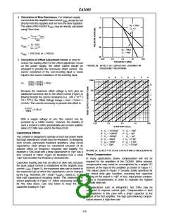
The high output impedance of the OTAs makes the CA3060
ideally suited for use as a gyrator in active filter applications.
Figure 24 shows two OTAs of the CA3060 connected as a
gyrator in an active filter circuit. The OTAs in this circuit can
make a 3µF capacitor function as a floating 10kH inductor
across Terminals A and B. The measured Q of 13 (at a
frequency of 1Hz) of this inductor compares favorably with a
calculated Q of 16. The 20kΩ to 2MΩ attenuators in this
circuit extend the dynamic range of the OTA by a factor of
100. The 100kΩ potentiometer, across V+ and V-, tunes the
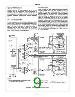
TRI-LEVEL
DETECTOR
V+
UPPER LIMIT
REFERENCE
VOLTAGE
SET
CA3086
POSITIVE
OUTPUT
-
+
FLIP-FLOP
(WHEN UPPER
LIMIT IS
INPUT
SIGNAL
RESET
+
-
REACHED)
INTERMEDIATE
LIMIT REFER-
ENCE VOLTAGE
V+
SET
CA3086
FLIP-FLOP
POSITIVE
OUTPUT
+
-
LOWER LIMIT
REFERENCE
VOLTAGE
inductor by varying the g of the OTAs, thereby changing
21
(WHEN LOWER
LIMIT IS
REACHED)
the gyration resistance.
V-
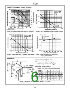
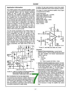
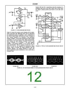
Three Channel Multiplexer
FIGURE 23. FUNCTIONAL BLOCK DIAGRAM OF A TRI-LEVEL
COMPARATOR
Figure 25 shows a schematic of a three channel multiplexer
using a single CA3060 and a 3N153 MOSFET as a buffer
and power amplifier.
The circuit diagram of a tri-level comparator appears in Figure
22. Power is provided for the CA3060 via terminal 3 and 8 by
±6V supplies and the built-in regulator provides amplifier bias
current (I
) to the three amplifiers via terminal 1. Lower
ABC
V+ = 15V
V+ = 15V
limit and upper limit reference voltages are selected by appro-
priate adjustment of potentiometers R and R , respectively.
When resistors R and R are equal in value (as shown), the
intermediate limit reference voltage is automatically estab-
lished at a value midway between the lower limit and upper
limit values. Appropriate variation of resistors R and R per-
mits selection of other values of intermediate limit voltage.
Input signal (E ) is applied to the three comparators via termi-
nals 5, 12 and 14. The “SET” output lines trigger the appropri-
ate flip-flop whenever the input signal reaches a limit value.
When the input signal returns to an intermediate value, the
common flip-flop “RESET” line is energized. The loads in the
circuits, shown in Figure 22 are 5V, 25mA lamps.
1
2
0.01µF
3
4
3
2kΩ
4
5
-
7
2kΩ
3
4
+
8
6
S
0.02
300kΩ
µF
V- = -15V
STROBE
3N153
2kΩ
12
11
-
9
3
4
2
2kΩ
+
V+ = 6V
390Ω
3
AMP 1
15
TERMINAL
A
10
0.001µF
20kΩ
20kΩ
300kΩ
14
13
STROBE
16
OUTPUT
2kΩ
3kΩ
13
14
-
16
2kΩ
V+
V-
+
560kΩ
V- = -15V
20
kΩ
20
kΩ
15
100kΩ
2MΩ
L = 10kH
+15V STROBE “ON”
-15V STROBE “OFF”
300kΩ
560kΩ
STROBE
10
3µF
FIGURE 25. THREE CHANNEL MULTIPLEXER
12
11
When the CA3060 is connected as a high input impedance
voltage follower, and strobe “ON”, each amplifier is activated
and the output swings to the level of the input of the
amplifier. The cascade arrangement of each CA3060
amplifier with the MOSFET provides an open loop voltage
gain in excess of 100dB, thus assuring excellent accuracy in
the voltage follower mode with 100% feedback. Operation at
±6V is also possible with several minor changes. First, the
9
AMP 2
8
2MΩ
TERMINAL
B
V- = -6V
resistance in series with the amplifier bias current (I
) ter-
ABC
FIGURE 24. TWO OPERATIONAL TRANSCONDUCTANCE
AMPLIFIERS OF THE CA3060 CONNECTED AS A
GYRATOR IN AN ACTIVE FILTER CIRCUIT
minal of each amplifier should be decreased to maintain
100µA of strobe “ON” current at this lower supply voltage.
Second, the drain resistance for the MOSFET should be
3-10

 HARRIS [ HARRIS CORPORATION ]