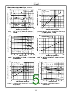
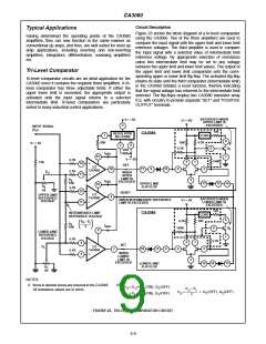
CA3060
o
Electrical Specifications
T = 25 C, V
SUPPLY
= ±15V (Continued)
A
AMPLIFIER BIAS CURRENT
= 10µA
I
= 1µA
I
I
= 100µA
ABC
ABC
ABC
PARAMETER
SYMBOL
MIN
TYP
MAX
MIN
TYP
MAX
MIN
TYP
MAX
UNITS
Input Impedance Components
Resistance (See Figure 14)
R
C
-
-
1600
2.7
-
-
-
-
170
2.7
-
-
10
-
20
-
-
kΩ
I
I
Capacitance at 1MHz
2.7
pF
Output Impedance Components
Resistance (See Figure 15)
R
C
-
-
200
4.5
-
-
-
-
20
-
-
-
-
2
-
-
MΩ
O
Capacitance at 1MHz
4.5
4.5
pF
O
ZENER BIAS REGULATOR CHARACTERISTICS I = 0.1mA
2
Voltage (See Figure 16)
V
Temperature
Coefficient = 3mV/ C
6.2
-
6.7
7.9
V
Z
o
Impedance
NOTES:
Z
200
300
Ω
Z
3. Conditions for Input Offset Voltage Sensitivity:
a. Bias current derived from the regulator with an appropriate resistor connected from Terminal 1 to the bias terminal on the amplifier
under test V+ is reduced to +13V for V+ sensitivity and V- is reduced to -13V for V- sensitivity.
V
– V
Offset
µV ⁄ V = ------------------------------------------------------------------------------------------------------------------------------ ,
for +13V and -15V Supplies
Offset
b. V+ Sensitivity in
1V
V
– V
Offset
V- Sensitivity in µV ⁄ V = ------------------------------------------------------------------------------------------------------------------------------.
for -13V and +15V Supplies
Offset
1V
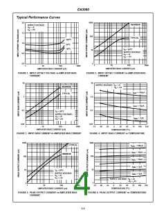
= 1µA); -2.1mV/ C (at V
o
o
o
4. Temperature Coefficient; -2.2mV/ C (at V
ABC
= 0.54, I
ABC
= 0.060V, I
ABC
= 10µA); -1.9mV/ C (at V = 0.66V,
ABC
ABC
I
= 100µA)
ABC
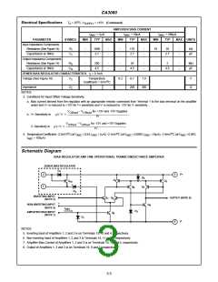
Schematic Diagram
BIAS REGULATOR AND ONE OPERATIONAL TRANSCONDUCTANCE AMPLIFIER
ZENER BIAS REGULATOR
D
4
V+
2
1
3
D
2
Q
4
Q
Q
5
10
Q
Q
7
6
D
5
-
INVERTING INPUT
(NOTE 5)
Q
Q
OUTPUT (NOTE 8)
1
2
+
NON-INVERTING INPUT
(NOTE 6)
Q
8
I
ABC
D
3
AMPLIFIER BIAS INPUT
(NOTE 7)
Q
3
D
1
V-
8
NOTES:
5. Inverting Input of Amplifiers 1, 2 and 3 is on Terminals 13, 12 and 4, respectively.
6. Non-inverting Input of Amplifiers 1, 2 and 3 is Terminals 14, 11 and 5, respectively.
7. Amplifier Bias Current of Amplifiers 1, 2 and 3 is on Terminals 15, 10 and 6, respectively.
8. Output of Amplifiers 1, 2 and 3 is on Terminals 16, 9 and 7, respectively.
3-3

 HARRIS [ HARRIS CORPORATION ]