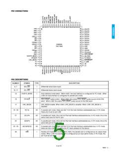
PIN CONNECTIONS
80 79 78 77 76 75 74 73 72 71 70 69 68 67 66 65 64 63 62 61
60
VDD
GND
GND
VDD
1
DOUT9
DOUT8
DOUT7
DOUT6
DOUT5
DOUT4
DOUT3
DOUT2
DOUT1
VDD
2
59
58
57
56
55
54
53
52
51
50
49
48
47
46
45
44
43
42
41
3
4
VDD
5
SDI
SDI
6
SDI
7
VDD
8
SDI
VDD
9
GS9020A
SCI
10
11
12
13
14
15
16
17
18
19
20
SCI
SCI
TOP VIEW
GND
VDD
DOUT0
PCLKOUT
FIFO_RESET
NO_EDH
FLYWDIS
INTERRUPT
F_R/W
SCI
VDD
GND
HOSTIF_MODE
FIFOE/S
CRC_MODE
P7
P6
P5
S0
S1
21 22 23 24 25 26 27 28 29 30 31 32 33 34 35 36 37 38 39 40
PIN DESCRIPTIONS
NUMBER
6, 7
SYMBOL
SDI, SDI
TYPE
DESCRIPTION
I
I
I
Differential serial data inputs.
Differential serial clock inputs.
10, 11
15
SCI, SCI
HOSTIF_MODE
Host interface mode select. When HIGH, the host interface is configured for I²C mode. When
LOW, the host interface is configured for parallel port mode.
16
17
FIFOE/S
CRC_MODE
P[7:5]
I
FIFO_RESET pulse control. When HIGH, the output FIFO_RESET pulse occurs on the EAV
word. When LOW, the output FIFO_RESET pulse occurs on the SAV word.
I
CRC_MODE enable. When HIGH, CRC_MODE is enabled. When LOW, CRC_MODE is
disabled.
18 - 20
21
I/O
I/O
I/O
I/O
I
In parallel port mode, these are bits 7:5 of the host interface address/data bus. In I²C mode,
these pins must be set LOW.
SCL/P4
In parallel port mode, this is bit 4 of the host interface address/data bus. In I²C mode, this is the
serial clock input for the I²C port.
22
SDA/P3
In parallel port mode, this is bit 3 of the host interface address/data bus. In I²C mode, this is the
serial data pin for the I²C port.
23 - 25
26
A[2:0]/P[2:0]
R/W
In parallel port mode, these are bits 2:0 of the host interface address/data bus. In I²C mode,
these are input bits which define the I²C slave address for the device.
Parallel port read/write control. When HIGH, the parallel port is configured as an output (read
mode). When LOW, the parallel port is configured as an input (write mode). In I²C mode, this
pin must be set HIGH.
5 of 31
19922 - 3

 GENNUM [ GENNUM CORPORATION ]