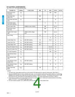
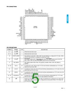
AC ELECTRICAL CHARCTERISTICS
VDD = 5.0 V, TA = 0 - 70°C unless otherwise shown.
PARAMETER
SYMBOL
CONDITIONS
MIN
TYP
MAX
UNITS
NOTES
Serial Input Clock
Frequency
ƒSCI
-
-
540
MHz
Serial Data Input
Setup Time
tSS
600
600
-
-
-
-
-
-
ps
ps
%
1
1
Serial Data Input Hold
Time
tSH
Serial Data Output
5
Duty Cycle Distortion
Serial Output Jitter
540Mb/s at eye crossing
-
-
360
600
-
-
ps p-p
ps
Serial Data Output
Rise Time
Parallel Clock Output
Jitter
27MHz at 50% voltage
level
-
700
-
ps p-p
Input Timing
t1
t2
20
-
-
-
-
-
-
-
-
-
-
ns
ns
2
2
3
3
3
-
9
Output Delay Time
Output Hold Time
tOD
tOH
tOS
tFDIS
tFEN
ƒSCL
tHS
with 25pF loading
with 25pF loading
with 25pF loading
with 25pF loading
with 25pF loading
T/2
T/2+7
ns
T/2-3
-
ns
Output Setup Time
Flag Port Disable Time
Flag Port Enable Time
I²C Clock Frequency
T/2-7
-
T/2+0.5
T/2+1
400
ns
-
-
ns
ns
-
kHz
ns
Host Interface Setup
Time
6
-
4
4
4
4
Host Interface Hold
Time
tHH
6
-
-
-
-
-
ns
ns
ns
ns
Host Interface Output
Enable Time
tHEN
with 25pF loading
with 25pF loading
-
-
21
10
-
Host Interface Output
Disable Time
tHDIS
Reset Time Pulse
Width
tRESET
100
NOTES
1. The serial clock rising edge should occur at the centre of the data period for optimum performance. (See Figure 1)
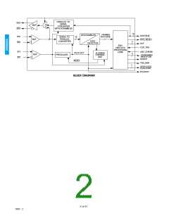
2. Since the GS9020A does not have a parallel clock input, it is not possible to define timing details relative to it. Instead the
GS9020A has a parallel clock output and all timing information is relative to PCLKOUT. The flag port pins (FL[4:0], F_R/W,
S[1:0]) are the only inputs where the timing details are important. The timing requirements are shown in Figure 2.
3. These times are relative to the rising edge of PCLKOUT as shown in Figure 3. Note that the data transitions at the falling
edge of PCLKOUT. T is the parallel clock period in ns.
4. The Host Interface signals, P[7:0], R/W, A/D and CS are asynchronous to the parallel clock.
4 of 31
19922 - 3

 GENNUM [ GENNUM CORPORATION ]