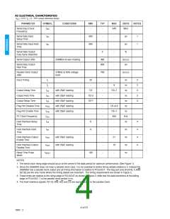
DETAILED DESCRIPTION
The GS9020A EDH coprocessor consists of five major
blocks:
SDI/SDI and SCI/SCI are high speed Pseudo-ECL (PECL)
compatible differential inputs with internal pullup resistors
(75Ω nominally) as shown in Figure 4. Note that each pullup
resistor has a dedicated power pin allowing the use of other
interfacing topologies.
1. Data Input/Output Block (with automatic standard
detect)
2. Flywheel Block
The internal pullup resistors allow the GS9020A to be easily
interfaced to the GS9025A as shown in Figure 5 and Figure
17. An external diode is required to offset the input signals
to the input range of the GS9020A. For maximum signal
integrity the GS9025A and GS9020A should be placed as
close together as possible.
3. EDH Block
4. Data Processing Block
5. Host Interface (HOSTIF) Block
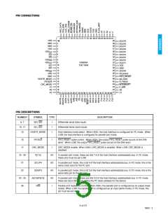
The following convention is used to differentiate device pins
from HOST interface table bits.
The PECL serial input signals are first converted to CMOS
levels and then deserialized to 10 bit parallel format (based
on the TRS headers), descrambled, and then passed to the
processing core.
PIN
LOGIC OPR
HOSTIF
XX
YY
1.2 Parallel Digital Video Data Outputs
LOGIC OPR (logic operator) gives the combinational
relationship (if one exists), between pins which also have a
corresponding HOST bit. This operator governs the signal
the GS9020A receives. The following is the list of possible
logic operators and their meaning.
PIN
LOGIC OPR
HOST BIT
DOUT[9:0]
The output of the device is 10-bit digital video data and is
present on the DOUT[9:0] output pins.
LOGIC OPR
MEANING
XX AND YY
1.3 Reserialized Data Output
AND
OR
>
XX OR YY
PIN
LOGIC OPR
HOST BIT
XX takes precedence over YY
YY takes precedence over XX
SDO, SDO
SDOMODE
<
1. DATA INPUT/OUTPUT BLOCK
1.1 Serial Video Data Inputs
The GS9020A also provides PECL differential serial data
outputs (SDO/SDO). The serial data outputs can operate in
one of two modes as controlled by the SDOMODE pin.
When SDOMODE is set LOW, re-serialized processed data
is output at the SDO/SDO output pins. In this mode it is
recommended that the lock output of the GS9025A or
GS9035A connected to the RESET input of the GS9020A,
and to a pull up resistor. This will effectively reset the
GS9020A whenever the signal lock is lost. Note that any
GS9020A programming through the host interface will be
lost after this reset. It will be necessary to reprogram the
GS9020A after each reset.
PIN
LOGIC OPR
HOST BIT
SDI, SDI
SCI, SCI
Serial data and clock signals are supplied to the GS9020A
chip via the SDI/SDI and SCI/SCI pins, respectively. Eight
standards are supported: Composite, 4:2:2 Component with
13.5MHz Y sampling, 4:2:2 16 x 9 wide screen with 18MHz
Y sampling, and 4:4:4:4 Component Single Link with
13.5MHz Y sampling, all in both NTSC and PAL formats.
See Table 1.
When SDOMODE is set HIGH, the serial input data is
supplied directly to the SDO/SDO output pins, bypassing
the processing core. After changing SDOMODE, the
GS9020A must be reset for proper operation.
8 of 31
19922 - 3

 GENNUM [ GENNUM CORPORATION ]