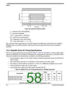
RapidIO
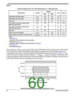
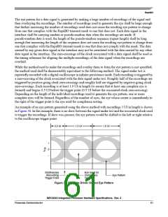
13.3.2 RapidIO Receiver AC Timing Specifications
The RapidIO receiver AC timing specifications are provided in Table 50. A receiver shall comply with the
specifications for each data rate/frequency for which operation of the receiver is specified. Unless
otherwise specified, these specifications are subject to the following conditions.
•
The specifications apply over the supply voltage and ambient temperature ranges specified by the
device vendor.
•
•
•
•
The specifications apply for any combination of data patterns on the data signals.
The specifications apply over the receiver common mode and differential input voltage ranges.
Clock specifications apply only to clock signals.
Data specifications apply only to data signals (FRAME, D[0:7])
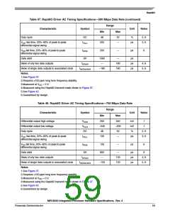
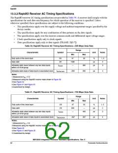
Table 50. RapidIO Receiver AC Timing Specifications—500 Mbps Data Rate
Range
Characteristic
Symbol
Unit
Notes
Min
Max
Duty cycle of the clock input
Data valid
DC
DV
47
1080
—
53
%
ps
ps
1, 5
2
Allowable static skew between any two data inputs
within a 8-/9-bit group
tDPAIR
380
300
3
Allowable static skew of data inputs to associated clock
tSKEW,PAIR
–300
ps
4
Notes:
1.Measured at VID = 0 V.
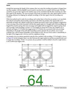
2.Measured using the RapidIO receive mask shown in Figure 39.
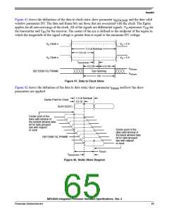
3.See Figure 42.
4.See Figure 41 and Figure 42.
5.Guaranteed by design.
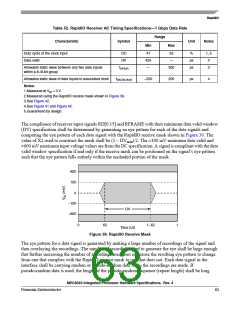
Table 51. RapidIO Receiver AC Timing Specifications—750 Mbps Data Rate
Range
Characteristic
Symbol
Unit
Notes
Min
Max
Duty cycle of the clock input
DC
DV
47
600
—
53
—
%
ps
ps
1, 5
2
Data valid
Allowable static skew between any two data inputs
within a 8-/9-bit group
tDPAIR
400
3
Allowable static skew of data inputs to associated clock
tSKEW,PAIR
–267
267
ps
4
Notes:
1.Measured at VID = 0 V.
2.Measured using the RapidIO receive mask shown in Figure 39.
3.See Figure 42.
4.See Figure 41 and Figure 42.
5.Guaranteed by design.
MPC8540 Integrated Processor Hardware Specifications, Rev. 4
62
Freescale Semiconductor

 FREESCALE [ Freescale ]