RapidIO
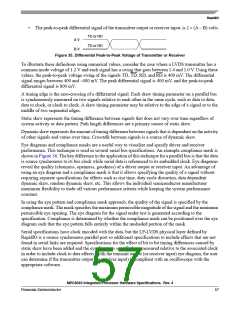
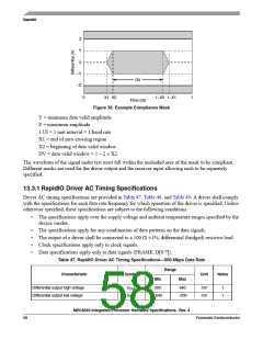
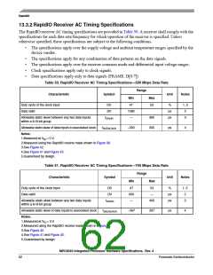
Z
Y
0
–Y
–Z
DV
0
X1 X2
1–X2 1–X1
1
Time (UI)
Figure 36. Example Compliance Mask
Y = minimum data valid amplitude
Z = maximum amplitude
1 UI = 1 unit interval = 1/baud rate
X1 = end of zero crossing region
X2 = beginning of data valid window
DV = data valid window = 1 – 2 × X2
The waveform of the signal under test must fall within the unshaded area of the mask to be compliant.
Different masks are used for the driver output and the receiver input allowing each to be separately
specified.
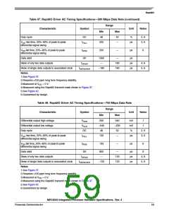
13.3.1 RapidIO Driver AC Timing Specifications
Driver AC timing specifications are provided in Table 47, Table 48, and Table 49. A driver shall comply
with the specifications for each data rate/frequency for which operation of the driver is specified. Unless
otherwise specified, these specifications are subject to the following conditions.
•
The specifications apply over the supply voltage and ambient temperature ranges specified by the
device vendor.
•
•
•
•
The specifications apply for any combination of data patterns on the data signals.
The output of a driver shall be connected to a 100 Ω, ±1%, differential (bridged) resistive load.
Clock specifications apply only to clock signals.
Data specifications apply only to data signals (FRAME, D[0:7]).
Table 47. RapidIO Driver AC Timing Specifications—500 Mbps Data Rate
Range
Characteristic
Symbol
Unit
Notes
Min
Max
Differential output high voltage
Differential output low voltage
VOHD
VOLD
200
540
mV
mV
1
1
–540
–200
MPC8540 Integrated Processor Hardware Specifications, Rev. 4
58
Freescale Semiconductor

 FREESCALE [ Freescale ]