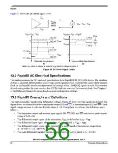
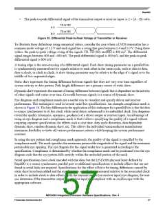
RapidIO
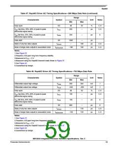
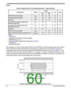
Table 49. RapidIO Driver AC Timing Specifications—1 Gbps Data Rate
Range
Characteristic
Symbol
Unit
Notes
Min
Max
Differential output high voltage
Differential output low voltage
Duty cycle
VOHD
VOLD
DC
200
–540
48
540
–200
52
mV
mV
%
1
1
2, 6
3, 6
VOD rise time, 20%–80% of peak to peak
differential signal swing
tFALL
100
—
ps
VOD fall time, 20%–80% of peak to peak
differential signal swing
tRISE
100
—
ps
6
Data valid
DV
575
—
—
ps
ps
ps
6
Skew of any two data outputs
Skew of single data outputs to associated clock
tDPAIR
100
100
4, 6
5, 6
tSKEW,PAIR
–100
Notes:
1.See Figure 37.
2.Requires 100 ppm long term frequency stability.
3.Measured at VOD = 0 V.
4.Measured using the RapidIO transmit mask shown in Figure 37.
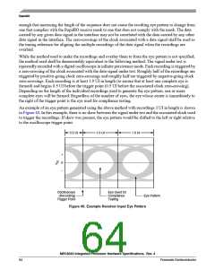
5.See Figure 42.
6.Guaranteed by design.
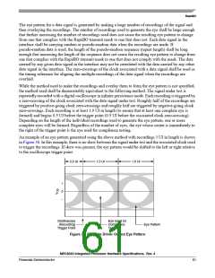
The compliance of driver output signals TD[0:15] and TFRAME with their minimum data valid window
(DV) specification shall be determined by generating an eye pattern for each of the data signals and
comparing the eye pattern of each data signal with the RapidIO transmit mask shown in Figure 37. The
value of X2 used to construct the mask shall be (1 – DV )/2. A signal is compliant with the data valid
min
window specification if the transmit mask can be positioned on the signal’s eye pattern such that the eye
pattern falls entirely within the unshaded portion of the mask.
VOHDmax
VOHDmin
0
VOLDmax
DV
VOLDmin
0
X2
1–X2
1
Time (UI)
Figure 37. RapidIO Transmit Mask
MPC8540 Integrated Processor Hardware Specifications, Rev. 4
60
Freescale Semiconductor

 FREESCALE [ Freescale ]