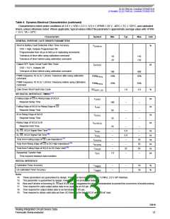
ELECTRICAL CHARACTERISTICS
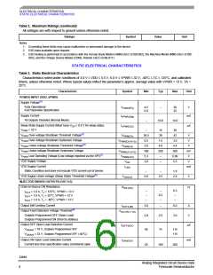
STATIC ELECTRICAL CHARACTERISTICS
Table 3. Static Electrical Characteristics
Characteristics noted under conditions of 3.0 V ≤ VDD ≤ 5.5 V, 6.0 V ≤ VPWR ≤ 32 V, -40°C ≤ TC ≤ 125°C, and calibrated
timers, unless otherwise noted. Where typical values reflect the parameter’s approx. average value with VPWR = 13 V, TA =
25°C.
Characteristic
Symbol
Min
Typ
Max
Unit
Notes
10. This parameter is guaranteed by design, however is not production tested.
11. Assuming Ideal external 10:1 Voltage Divider. Tolerance of 10:1 Voltage Divider is not included. Voltage is measured on the High End
of Divider - not at the pin. 10:1 N.3.A 10:1 Voltage Divider is produced using two resistors with a 9:1 resistance ratio by the basic formula:
VOUT
VIN
R1
R1 + R2
----------------------
----------------- =
Where R2 = 9XR1
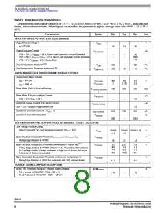
CURRENT SENSE COMPARATOR (RSP, RSN) (CONTINUED)
MAXI Trip Threshold Accuracy
7.5
%
Steady State Condition
6.0 A across 0.02 Ω (RSP - RSN = 120 mV)
21 A across 0.04 Ω (RSP - RSN = 840 mV)
MAXI
MAXI
–
TRIPTA
-7.5
-35
MAXI Trip Point During Overlapping Dwell
–
–
+35
50
%
TRIPOD
Input Bias Current
RSP and RSN
I
µA
BIASRSX
-50
Comparator Hysteresis Voltage
NOMI
MAXI
NOMI
MAXII
40
40
–
–
70
70
% of VT
HYS
HYS
Input Voltage Range (Maximum voltage between RSN and RSP)(12)
VCMVR
VGND
0.0
–
–
2.0
0.3
V
V
CMVR
Ground Offset Voltage Range(12)
-0.3
OVR
Maximum offset between RSN pin and IC Ground (Exposed Pad)
GENERAL PURPOSE GATE DRIVER PARAMETERS (GD 0:3)
Gate Drive Sink and Source Current
IGD
1.0
2.0
5
mA
Gate Drive Output Voltage
IGD = 1.0 mA
V
4.8
0.0
7.0
0.2
9.0
0.5
V
V
GS(ON)
V
IGD = -1.0 mA
GS(OFF)
Short to Battery Fault Detection Voltage Threshold
V
V
DS(FLT-TH)
V
= 5.0 V, Outputs Programmed ON
-35%
2.0
+35%
3.0
DD
Programmable from 0.5 to 3.0 V in 0.5 V increments. (Table 14)
Open Fault Detection Voltage Threshold (referenced to IC ground tab)
V
V
DS(FLT-TH)
V
= 5.0 V, Outputs Programmed OFF
2.5
DD
Output OFF Open Load Detection Current
FBx = 18 V, Outputs Programmed OFF
I
μA
FBX(FLT-SNS)
50
48
75
53
120
58
Output Clamp Voltage
V
V
OC
Driver Command Off, Clamp Enabled, VGATE = 2.0 V
DIGITAL INTERFACE
Input Logic High-voltage Thresholds
Input Logic Low-voltage Thresholds
Input Logic-voltage Hysteresis
Input Logic Capacitance
V
0.7 x VDD
GND - 0.3
100
–
–
–
–
VDD + 0.3
0.2 x VDD
400
V
V
IH
V
IL
V
mV
pF
μA
HYS
C
–
20
IN
LOGIC_SS
Sleep Mode Input Logic Current
I
V
= 0 V
-10
–
10
DD
33810
Analog Integrated Circuit Device Data
Freescale Semiconductor
9

 FREESCALE [ Freescale ]