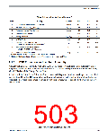
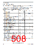
Electrical Characteristics
P is the sum of all output currents on I/O ports associated with V
, whereby
IO
DDX
V
OL
R
= -----------;for outputs driven low
DSON
I
OL
V
– V
DD35
OH
R
= --------------------------------------;for outputs driven high
DSON
P
I
OH
= I
⋅ V
+ I
⋅ V
INT
DDR DDR DDA DDA
(1)
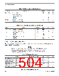
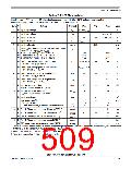
Table A-5. Thermal Package Characteristics
Num
C
Rating
Symbol
Min
Typ
Max
Unit
QFN 48
1
2
D
D
Thermal resistance QFN 48, single sided PCB(2)
θJA
θJA
—
—
—
—
82
28
°C/W
°C/W
Thermal resistance QFN 48, double sided PCB
with 2 internal planes(3)
3
4
5
D
D
D
Junction to Board QFN 48
θJB
θJC
ΨJT
—
—
—
—
—
—
11
1.4
4
°C/W
°C/W
°C/W
Junction to Case QFN 484
Junction to Case (Bottom) QFN 485
QFP 80
6
7
D
D
Thermal resistance QFP 80, single sided PCB2
θJA
θJA
—
—
—
—
56
43
°C/W
°C/W
Thermal resistance QFP 80, double sided PCB
with 2 internal planes3
8
9
D
D
D
Junction to Board QFP 80
θJB
θJC
ΨJT
—
—
—
—
—
—
28
19
5
°C/W
°C/W
°C/W
Junction to Case QFP 80(4)
Junction to Package Top QFP 80(5)
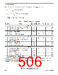
10
LQFP 64
11
12
D
D
Thermal resistance LQFP 64, single sided PCB2
θJA
θJA
—
—
—
—
70
52
°C/W
°C/W
Thermal resistance LQFP 64, double sided PCB
with 2 internal planes3
13
14
15
D
D
D
Junction to Board LQFP 64
θJB
θJC
ΨJT
—
—
—
—
—
—
35
17
3
°C/W
°C/W
°C/W
Junction to Case LQFP 64(6)
Junction to Package Top LQFP 64(7)
1. The values for thermal resistance are achieved by package simulations
2. Junction to ambient thermal resistance, θJA was simulated to be equivalent to the JEDEC specification JESD51-2 in a
horizontal configuration in natural convection.
3. Junction to ambient thermal resistance, θJA was simulated to be equivalent to the JEDEC specification JESD51-7 in a
horizontal configuration in natural convection.
S12P-Family Reference Manual, Rev. 1.13
506
Freescale Semiconductor

 FREESCALE [ Freescale ]