Electrical Characteristics
(1)
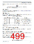
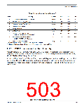
Table A-1. Absolute Maximum Ratings
Num
Rating
Symbol
Min
Max
Unit
1
2
3
4
5
6
7
I/O, regulator and analog supply voltage
Voltage difference VDDX to VDDA
Voltage difference VSSX to VSSA
Digital I/O input voltage
VDD35
–0.3
–6.0
–0.3
–0.3
–0.3
–0.3
–25
6.0
0.3
V
V
∆
VDDX
∆
0.3
V
VSSX
VIN
VRH, VRL
VILV
6.0
V
Analog reference
6.0
V
EXTAL, XTAL
2.16
+25
V
Instantaneous maximum current
ID
mA
Single pin limit for all digital I/O pins(2)
8
Instantaneous maximum current
Single pin limit for EXTAL, XTAL
IDL
–25
–65
+25
155
mA
9
Storage temperature range
T
°C
stg
1. Beyond absolute maximum ratings device might be damaged.
2. All digital I/O pins are internally clamped to VSSX and VDDX, or VSSA and VDDA
.
A.1.6
ESD Protection and Latch-up Immunity
All ESD testing is in conformity with CDF-AEC-Q100 stress test qualification for automotive grade
integrated circuits. During the device qualification ESD stresses were performed for the Human Body
Model (HBM) and the Charge Device Model.
A device will be defined as a failure if after exposure to ESD pulses the device no longer meets the device
specification. Complete DC parametric and functional testing is performed per the applicable device
specification at room temperature followed by hot temperature, unless specified otherwise in the device
specification.
S12P-Family Reference Manual, Rev. 1.13
Freescale Semiconductor
503

 FREESCALE [ Freescale ]