Electrical Characteristics
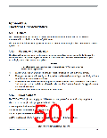
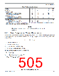
Table A-2. ESD and Latch-up Test Conditions
Description
Model
Human Body
Symbol
Value
Unit
Series resistance
Storage capacitance
R1
C
1500
100
Ohm
pF
Number of pulse per pin
Positive
—
—
3
3
Negative
Latch-up
Minimum input voltage limit
Maximum input voltage limit
—
—
–2.5
7.5
V
V
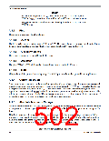
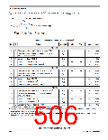
Table A-3. ESD and Latch-Up Protection Characteristics
Num
C
Rating
Symbol
Min
Max
Unit
1
2
3
C
C
C
Human Body Model (HBM)
Charge Device Model (CDM)
VHBM
VCDM
ILAT
2000
500
—
—
V
V
Latch-up current at TA = 125°C
mA
Positive
Negative
+100
–100
—
—
4
C
Latch-up current at TA = 27°C
ILAT
mA
Positive
+200
–200
—
—
Negative
A.1.7
Operating Conditions
This section describes the operating conditions of the device. Unless otherwise noted those conditions
apply to all the following data.
NOTE
Please refer to the temperature rating of the device (C, V, M) with regards to
the ambient temperature T and the junction temperature T . For power
A
J
dissipation calculations refer to Section A.1.8, “Power Dissipation and
Thermal Characteristics”.
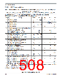
Table A-4. Operating Conditions
Rating
Symbol
Min
Typ
Max
Unit
I/O, regulator and analog supply voltage
Voltage difference VDDX to VDDA
Voltage difference VDDR to VDDX
Voltage difference VSSX to VSSA
Voltage difference VSS3 , VSSPLL to VSSX
Digital logic supply voltage
VDD35
3.13
5
5.5
V
∆
refer to Table A-14
VDDX
∆
-0.1
0
0.1
V
VDDR
∆
refer to Table A-14
VSSX
∆
-0.1
0
0.1
1.98
V
V
VSS
VDD
1.72
1.8
S12P-Family Reference Manual, Rev. 1.13
504
Freescale Semiconductor

 FREESCALE [ Freescale ]