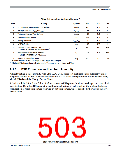
Electrical Characteristics
NOTE
In the following context V
is used for either VDDA, VDDR, and
DD35
VDDX; V
is used for either VSSA and VSSX unless otherwise noted.
SS35
I
denotes the sum of the currents flowing into the VDDA, VDDX and
DD35
VDDR pins.
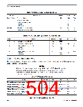
A.1.3
Pins
There are four groups of functional pins.
A.1.3.1
I/O Pins
The I/O pins have a level in the range of 3.15V to 5.5V. This class of pins is comprised of all port I/O pins,
the analog inputs, BKGD and the RESET pins. Some functionality may be disabled.
A.1.3.2
Analog Reference
This group is made up by the VRH and VRL pins.
A.1.3.3
Oscillator
The pins EXTAL, XTAL dedicated to the oscillator have a nominal 1.8V level.
A.1.3.4
TEST
This pin is used for production testing only. The TEST pin must be tied to ground in all applications.
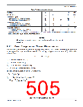
A.1.4
Current Injection
Power supply must maintain regulation within operating V
or V range during instantaneous and
DD
DD35
operating maximum current conditions. If positive injection current (V > V
) is greater than I
,
in
DD35
DD35
the injection current may flow out of V
and could result in external power supply going out of
DD35
regulation. Ensure external V
load will shunt current greater than maximum injection current. This
DD35
will be the greatest risk when the MCU is not consuming power; e.g., if no system clock is present, or if
clock rate is very low which would reduce overall power consumption.
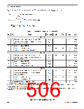
A.1.5
Absolute Maximum Ratings
Absolute maximum ratings are stress ratings only. A functional operation under or outside those maxima
is not guaranteed. Stress beyond those limits may affect the reliability or cause permanent damage of the
device.
This device contains circuitry protecting against damage due to high static voltage or electrical fields;
however, it is advised that normal precautions be taken to avoid application of any voltages higher than
maximum-rated voltages to this high-impedance circuit. Reliability of operation is enhanced if unused
inputs are tied to an appropriate logic voltage level (e.g., either V
or V
).
SS35
DD35
S12P-Family Reference Manual, Rev. 1.13
502
Freescale Semiconductor

 FREESCALE [ Freescale ]