128 KByte Flash Module (S12FTMRC128K1V1)
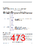
Table 13-64. Erase D-Flash Sector Command Error Handling
Register
Error Bit
Error Condition
Set if CCOBIX[2:0] != 001 at command launch
Set if command not available in current mode (see Table 13-27)
Set if an invalid global address [17:0] is supplied
ACCERR
Set if a misaligned word address is supplied (global address [0] != 0)
Set if the selected area of the D-Flash memory is protected
Set if any errors have been encountered during the verify operation
FSTAT
FPVIOL
MGSTAT1
Set if any non-correctable errors have been encountered during the verify
operation
MGSTAT0
13.4.6 Interrupts
The Flash module can generate an interrupt when a Flash command operation has completed or when a
Flash command operation has detected an ECC fault.
Table 13-65. Flash Interrupt Sources
Global (CCR)
Interrupt Source
Interrupt Flag
Local Enable
Mask
Flash Command Complete
CCIF
CCIE
I Bit
(FSTAT register)
(FCNFG register)
ECC Double Bit Fault on Flash Read
ECC Single Bit Fault on Flash Read
DFDIF
(FERSTAT register)
DFDIE
(FERCNFG register)
I Bit
I Bit
SFDIF
SFDIE
(FERSTAT register)
(FERCNFG register)
NOTE
Vector addresses and their relative interrupt priority are determined at the
MCU level.
13.4.6.1 Description of Flash Interrupt Operation
The Flash module uses the CCIF flag in combination with the CCIE interrupt enable bit to generate the
Flash command interrupt request. The Flash module uses the DFDIF and SFDIF flags in combination with
the DFDIE and SFDIE interrupt enable bits to generate the Flash error interrupt request. For a detailed
description of the register bits involved, refer to Section 13.3.2.5, “Flash Configuration Register
(FCNFG)”, Section 13.3.2.6, “Flash Error Configuration Register (FERCNFG)”, Section 13.3.2.7, “Flash
Status Register (FSTAT)”, and Section 13.3.2.8, “Flash Error Status Register (FERSTAT)”.
The logic used for generating the Flash module interrupts is shown in Figure 13-27.
S12P-Family Reference Manual, Rev. 1.13
Freescale Semiconductor
469

 FREESCALE [ Freescale ]