Freescale Semiconductor, Inc.
Serial Communications Interface (SCI)
Functional Description
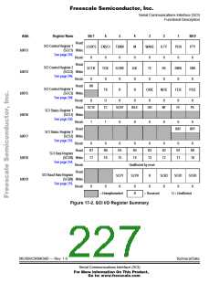
Addr.
Register Name
Bit 7
6
5
4
M
0
3
WAKE
0
2
ILTY
0
1
PEN
0
Bit 0
PTY
0
Read:
SCI Control Register 1
LOOPS ENSCI TXINV
$0013
(SCC1) Write:
See page 243.
Reset:
Read:
0
0
TCIE
0
0
SCRIE
0
SCI Control Register 2
SCTIE
ILIE
0
TE
RE
0
RWU
0
SBK
0
$0014
$0015
$0016
$0017
$0018
$0019
(SCC2) Write:
See page 246.
Reset:
Read:
0
0
R8
SCI Control Register 3
T8
R
R
ORIE
NEIE
FEIE
PEIE
(SCC3) Write:
See page 248.
Reset:
U
U
0
0
0
0
0
0
Read: SCTE
TC
SCRF
IDLE
OR
NF
FE
PE
SCI Status Register 1
(SCS1) Write:
See page 250.
Reset:
Read:
1
1
0
0
0
0
0
0
BKF
RPF
SCI Status Register 2
(SCS2) Write:
See page 253.
Reset:
Read:
0
0
0
0
0
0
0
0
R7
T7
R6
T6
R5
T5
R4
T4
R3
T3
R2
T2
R1
T1
R0
T0
SCI Data Register
(SCDR) Write:
See page 254.
Reset:
Read:
Unaffected by reset
SCI Baud Rate Register
SCP1
0
SCP0
R
SCR2
0
SCR1
0
SCR0
0
(SCBR) Write:
See page 255.
Reset:
0
0
0
0
= Unimplemented
R
= Reserved
U = Unaffected
Figure 17-2. SCI I/O Register Summary
MC68HC908AS60 — Rev. 1.0
Technical Data
Serial Communications Interface (SCI)
For More Information On This Product,
Go to: www.freescale.com

 FREESCALE [ Freescale ]