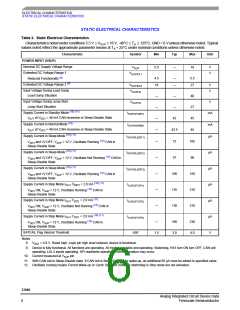
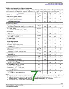
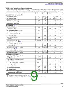
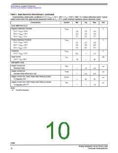
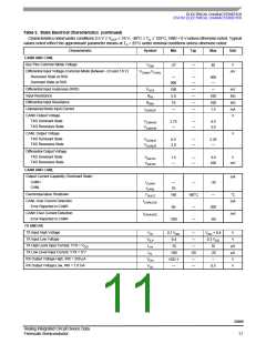
ELECTRICAL CHARACTERISTICS
STATIC ELECTRICAL CHARACTERISTICS
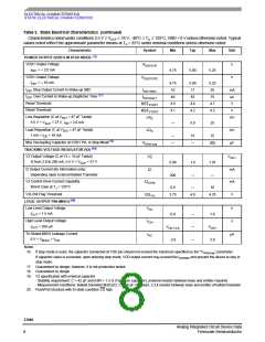
Table 3. Static Electrical Characteristics (continued)
Characteristics noted under conditions 5.5 V ≤ VSUP ≤ 18 V, -40°C ≤ TA ≤ 125°C, GND = 0 V unless otherwise noted. Typical
values noted reflect the approximate parameter means at TA = 25°C under nominal conditions unless otherwise noted.
Characteristic
BATFAIL Flag Hysteresis (13)
Symbol
VBF
Min
Typ
Max
Unit
—
1.0
—
V
V
(HYS)
Battery Fall Early Warning Threshold
In Normal and Standby Mode
BF
EW
5.3
0.1
5.8
0.2
6.3
0.3
Battery Fall Early Warning Hysteresis
In Normal and Standby Mode (13)
POWER OUTPUT (VDD1) (14)
VDD1 Output Voltage
BF
V
EWH
V
V
V
V
V
DD1OUT
I
from 2.0 to 200 mA T
-40 to 125°C, 5.5 V < VSUP < 27 V
4.9
4.0
—
5.0
—
5.1
—
DD1
AMB
VDD1 Output Voltage
from 2.0 to 200 mA, 4.5 V < VSUP < 5.5 V
V
DD1OUT2
I
DD1
Dropout Voltage
= 200 mA
V
DD1DRP
I
0.2
0.1
0.5
0.25
DD1
Dropout Voltage, Limited Output Current
V
DD1DRP2
I
= 50 mA, 4.5 V < VSUP
—
DD1
I
Output Current
I
mA
°C
DD1
DD1
Internally Limited
200
160
285
—
350
200
Junction Thermal Shutdown
Normal or Standby Modes
T
SD
Junction Over Temperature Pre-Warning
°C
T
PW
- T
V
Bit Set
125
20
—
—
160
40
DDTEMP
Temperature Threshold Difference
T
°C
V
SD
PW
Reset Threshold 1
RST
TH1
Selectable by SPI. Default Value After Reset.
4.5
4.6
4.7
Reset Threshold 2
Selectable by SPI
V
RST
TH2
4.1
1.0
4.2
—
4.3
—
VDD1 Range for Reset Active
V
V
DDR
Reset Delay Time
—
µs
t
D
Measured at 50% of Reset Signal
4.0
—
30
25
Line Regulation (C at VDD1 = 47 µF Tantal)
9.0 V VSUP < 18, IDD = 10 mA
mV
mV
mV
mV
LR1
LR2
5.0
10
25
30
Line Regulation (C at VDD1 = 47 µF Tantal)
5.5 < VSUP < 27 V, IDD = 10 mA
—
25
75
50
Load Regulation (C at VDD1 = 47 µF Tantal)
1.0 mA < IIDD < 200 mA
LD
—
—
Thermal Stability
THERM
S
VSUP = 13.5 V, 1 = -100 mA Not Tested (15)
Notes
13. With CAN cell in Sleep-Disable state. If CAN cell is Sleep-Enabled for wake-up, an additional 60 µA must be added to specified value.
14. is the total regulator output current. V specification with external capacitor. Stability requirement: C > 47 µF ESR < 1.3 Ω
I
DD1
DD
(tantalum capacitor). In reset, normal request, normal and standby modes. Measure with C = 47 µF Tantalum.
15. Guaranteed by design; however, it is not production tested.
33989
Analog Integrated Circuit Device Data
Freescale Semiconductor
7

 FREESCALE [ Freescale ]