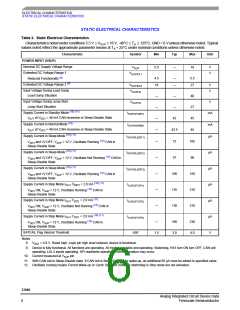
ELECTRICAL CHARACTERISTICS
STATIC ELECTRICAL CHARACTERISTICS
STATIC ELECTRICAL CHARACTERISTICS
Table 3. Static Electrical Characteristics
Characteristics noted under conditions 5.5 V ≤ VSUP ≤ 18 V, -40°C ≤ TA ≤ 125°C, GND = 0 V unless otherwise noted. Typical
values noted reflect the approximate parameter means at TA = 25°C under nominal conditions unless otherwise noted.
Characteristic
Symbol
Min
Typ
Max
Unit
POWER INPUT (VSUP)
Nominal DC Supply Voltage Range
Extended DC Voltage Range 1
Reduced Functionality (8)
V
5.5
—
18
V
V
SUP
V
V
SUPEX1
4.5
18
—
—
5.5
27
Extended DC Voltage Range 2 (9)
V
V
SUPEX2
Input Voltage During Load Dump
Load Dump Situation
V
SUPLD
—
—
—
—
—
42
40
27
45
Input Voltage During Jump Start
Jump Start Situation
V
V
SUPJS
Supply Current in Standby Mode (10) (11)
I
mA
SUP(STDBY)
I
at VDD1 = 40 mA CAN recessive or Sleep-Disable State
OUT
Supply Current in Normal Mode (10)
at VDD1 = 40 mA CAN recessive or Sleep-Disable State
I
mA
µA
SUP(NORM)
I
—
—
42.5
72
45
OUT
Supply Current in Sleep Mode (10) (11)
I
I
I
SUP(SLEEP1)
SUP(SLEEP2)
SUP(SLEEP3)
VDD1 and V2 OFF, VSUP < 12 V, Oscillator Running (12) CAN in
Sleep-Disable State
105
Supply Current in Sleep Mode (10) (11)
µA
µA
µA
µA
µA
V
VDD1 and V2 OFF, VSUP < 12 V, Oscillator Not Running (12) CAN in
Sleep-Disable State
—
—
—
—
57
90
Supply Current in Sleep Mode (10) (11)
VDD1 and V2 OFF, VSUP > 12 V, Oscillator Running (12) CAN in
Sleep-Disable State
100
135
130
150
210
210
Supply Current in Stop Mode IOUT VDD1 < 2.0 mA (10) (11)
I
I
I
SUP(STOP1)
SUP(STOP2)
VDD1 ON, VSUP < 12 V, Oscillator Running (12) CAN in
Sleep-Disable State
Supply Current in Stop Mode I
V
< 2.0 mA (11)
OUT DD1
VDD1 ON, VSUP < 12 V, Oscillator Not Running (12) CAN in
Sleep-Disable State
Supply Current in Stop Mode I
V
< 2.0 mA (10) (11)
OUT DD1
SUP(STOP3)
VBF
VDD1 ON, VSUP > 12 V, Oscillator Running (12) CAN in
Sleep-Disable State
—
160
3.0
230
4.0
BATFAIL Flag Internal Threshold
1.5
Notes
8. VDD1 > 4.0 V, Reset high, Logic pin high level reduced, device is functional.
9. Device is fully functional. All functions are operating. All modes available and operating. Watchdog, HS1 turn ON turn OFF, CAN cell
operating, L0:L3 inputs operating, SPI read/write operation. Overtemperature may occur.
10. Current measured at VSUP pin.
11. With CAN cell in Sleep-Disable state. If CAN cell is Sleep-Enabled for wake-up, an additional 60 µA must be added to specified value.
12. Oscillator running means Forced Wake-up or Cyclic Sense of Software Watchdog is Stop mode are not activated.
33989
Analog Integrated Circuit Device Data
Freescale Semiconductor
6

 FREESCALE [ Freescale ]