ELECTRICAL CHARACTERISTICS
STATIC ELECTRICAL CHARACTERISTICS
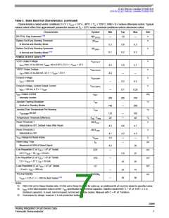
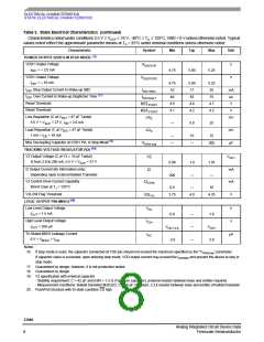
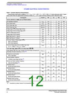
Table 3. Static Electrical Characteristics (continued)
Characteristics noted under conditions 5.5 V ≤ VSUP ≤ 18 V, -40°C ≤ TA ≤ 125°C, GND = 0 V unless otherwise noted. Typical
values noted reflect the approximate parameter means at TA = 25°C under nominal conditions unless otherwise noted.
Characteristic
Symbol
Min
Typ
Max
Unit
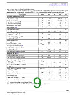
POWER OUTPUT (VDD1) IN STOP MODE (16)
VDD1 Output Voltage
IDD1 < = 2.0 mA
V
V
V
DDSTOP
DDSTOP2
DD1SWU
4.75
5.00
5.25
VDD1 Output Voltage
IDD1 < = 10 mA
V
4.75
10
5.00
17
5.25
25
IDD1 Stop Output Current to Wake-up SBC
IDD1 Over Current to Wake-up Deglitcher Time (17)
Reset Threshold
mA
µs
V
I
40
55
75
I
DD1DGLT
4.5
4.1
4.6
4.2
4.7
4.3
RST
RST
STOP1
STOP2
Reset Threshold
V
Line Regulation (C at VDD1 = 47 µF Tantal)
LR
mV
S
5.5 V < V
< 27 V, IDD = 2.0 mA
—
5.0
25
SUP
Load Regulation (C at VDD1 = 47 µF Tantal)
1 mA < IDD < 10 mA
LD
mV
µF
S
—
—
15
—
75
Max Decoupling Capacitor at VDD1 Pin, in Stop Mode(18)
200
V
DDst-cap
TRACKING VOLTAGE REGULATOR (V2) (19)
V2 Output Voltage (C at V2 = 10 µF Tantal)
V
V2
DD1
mA
mA
I2 from 2.0 to 200 mA, 5.5 V < V
< 27 V
0.99
200
1.0
—
1.01
—
SUP
I2 Output Current (for information only)
I2
Depending Upon External Ballast Transistor
V2 Control Drive Current Capability
12
CTRL
Worst Case at T = 125°C
J
0.0
—
10
V2LOW Flag Threshold
3.75
4.0
4.25
V
V2L
TH
LOGIC OUTPUT PIN (MISO) (20)
Low Level Output Voltage
V
V
V
OL
I
= 1.5 mA
0.0
—
—
—
1.0
OUT
High Level Output Voltage
= 250 µA
V
OH
HZ
I
V
V
OUT
DD1-0.9
-2.0
DD1
Tri-Stated MISO Leakage Current
0 V < V < V
I
µA
2.0
MISO
DD
Notes
16. If stop mode is used, the capacitor connected at VDD pin should not exceed the maximum specified by the “VDDst-cap” parameter.
If capacitor value is exceeded, upon entering stop mode, VDD output current may exceed the IDDSWU and prevent the device to stay in
stop mode.
17. Guaranteed by design; however, it is not production tested.
18. Guaranteed by design.
19. V2 specification with external capacitor
- Stability requirement: C > 42 µF and ESR < 1.3 Ω (Tantalum capacitor), external resistor between base and emitter required
- Measurement conditions: Ballast transistor MJD32C, C = 10 µF Tantalum, 2.2 k resistor between base and emitter of ballast transistor
20. Push/Pull structure with tri-state condition CS high.
33989
Analog Integrated Circuit Device Data
Freescale Semiconductor
8

 FREESCALE [ Freescale ]