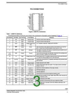
PIN CONNECTIONS
PIN CONNECTIONS
1
28
27
26
25
24
23
22
21
20
19
18
17
16
15
RX
TX
VDD1
RST
WD
CS
2
3
MOSI
MISO
SCLK
GND
GND
GND
GND
CANL
CANH
L3
4
5
INT
6
GND
GND
GND
GND
V2
7
8
9
10
11
12
13
14
V2CTRL
VSUP
HS1
L2
L1
L0
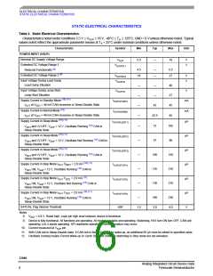
Figure 3. 33989 Pin Connections
Table 1. 33989 Pin Definitions
A functional description of each pin can be found in the Functional Pin Description section beginning on page 18.
Pin Number Pin Name Pin Function
Formal Name
Definition
CAN bus receive data output pin.
1
2
3
RX
TX
Output
Input
Receive Data
Transmit Data
CAN bus transmit data input pin.
5.0 V regulator output pin. Supply pin for the MCU.
VDD1
Power
Output
Voltage Digital Drain
One
This is the device reset output pin whose main function is to reset the
MCU. This pin has an internal pullup current source to VDD.
4
5
RST
INT
Output
Output
Ground
Input
Reset
Interrupt
This output is asserted LOW when an enabled interrupt condition occurs.
The output is a push-pull structure.
These device ground pins are internally connected to the package lead
frame to provide a 33989-to-PCB thermal path.
6–9
20–23
GND
V2
Ground
Sense input for the V2 regulator using an external series pass transistor.
V2 is also the internal supply for the CAN transceiver.
10
Voltage Source Two
Voltage Control
Output drive source for the V2 regulator connected to the external series
pass transistor.
11
V2CTRL
Power
Output
Supply input pin for the 33989.
12
13
VSUP
HS1
Power
Output
Voltage Supply
High Side One
Output of the internal high-side switch. The output current is internally
limited to 150 mA.
Inputs from external switches or from logic circuitry.
CAN high output pin.
14–17
22
L0:L3
CANH
CANL
SCLK
MISO
Input
Output
Output
Input
Level 0: 3
CAN High
CAN low output pin.
23
CAN Low
Clock input pin for the Serial Peripheral Interface (SPI).
24
System Clock
Master In/Slave Out
SPI data sent to the MCU by the 33989. When CS is HIGH, the pin is in
the high-impedance state.
25
Output
SPI data received by the 33989.
26
27
28
MOSI
CS
Input
Input
Master Out/Slave In
Chip Select
The CS input pin is used with the SPI bus to select the 33989.
The WD output pin is asserted LOW if the software watchdog is not
correctly triggered.
WD
Output
Watch Dog
33989
Analog Integrated Circuit Device Data
Freescale Semiconductor
3

 FREESCALE [ Freescale ]