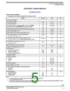
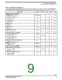
ELECTRICAL CHARACTERISTICS
MAXIMUM RATINGS
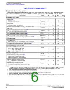
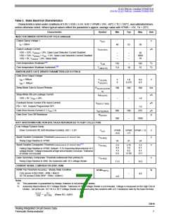
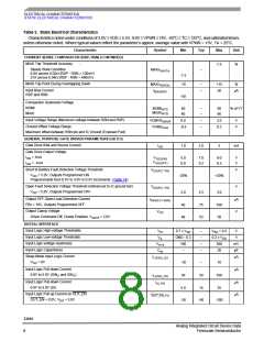
ELECTRICAL CHARACTERISTICS
MAXIMUM RATINGS
Table 2. Maximum Ratings
All voltages are with respect to ground unless otherwise noted.
Ratings
Symbol
Value
Unit
ELECTRICAL RATINGS
VPWR Supply Voltage(1)
VDD Supply Voltage(1)
V
-1.5 to 45
-0.3 to 7.0
-0.3 to VDD
V
V
V
PWR
DC
DC
DC
V
DD
SPI Interface and Logic Input Voltage (CS, SI, SO, SCLK, OUTEN,
DIN0 - DIN3, GIN0 - GIN3, SPKDUR, NOMI, MAXI, RSP,RSN)
VIL
VIH
IGBT/General Purpose Gate Pre-driver Drain Voltage (VFB0 to VFB3
Injector Output Voltage (OUTx)
)
VFB
-1.5 to 60
-1.5 to 60
-0.3 to 10
100
V
V
V
DC
DC
DC
V
OUTX
General Purpose Gate Pre-driver Output Voltage (GDx)
V
GDx
Output Clamp Energy (OUT0 to OUT3)(Single Pulse)
TJUNCTION = 150°C, IOUT = 1.5A
E
mJ
mJ
A
CLAMP
Output Clamp Energy (OUT0 to OUT3)(Continuous Pulse)
E
100
2.0
CLAMP
TJUNCTION = 125°C, IOUT = 1.0A (Max Injector frequency is 70Hz)
Output Continuous Current (OUT0 to OUT3)
TJUNCTION = 150°C
IOSSSS
Maximum Voltage for RSN and RSP inputs
Frequency of SPI Operation (VDD = 5.0V)
V
-0.3 - VDD
6.0
V
DC
RSX
–
MHz
ESD Voltage(2), (3)
V
VESD1
VESD2
VESD3
±2000
±200
±750
Human Body Model (HBM)
Machine Model (MM)
Charge Device Model (CDM)
THERMAL RATINGS
Operating Temperature
Ambient
°C
TA
TJ
-40 to 125
-40 to 150
-40 to 125
Junction2
Case
TC
Storage Temperature
T
-55 to 150
1.7
°C
W
STG
Power Dissipation (T = 25°C)
P
D
A
Peak Package flow Temperature During Solder Mounting
TSOLDER
°C
DWB Suffix
EW Suffix
240
245
Thermal Resistance
Junction-to-Ambient
Junction- to-Lead
Junction-to-Flag
°C/W
R
R
R
75
8.0
1.2
JA
θJL
θJC
θ
Notes
1. Exceeding these limits may cause malfunction or permanent damage to the device.
2. ESD data available upon request.
3. ESD testing is performed in accordance with the Human Body Model (HBM) (AEC-Q100-002), the Machine Model (MM) (AEC-Q100-
003), and the Charge Device Model (CDM), Robotic (AEC-Q100-011).
33810
Analog Integrated Circuit Device Data
Freescale Semiconductor
5

 FREESCALE [ Freescale ]