PIN CONNECTIONS
PIN CONNECTIONS
OUT2
FB2
GD2
MAXI
NOMI
RSN
OUT0
FB0
GD0
CS
SCLK
SI
SO
VDD
OUTEN
DIN0
DIN1
DIN2
DIN3
GD1
FB1
1
2
3
4
5
6
7
8
32
31
30
29
28
27
26
25
24
23
22
21
20
19
18
17
RSP
VPWR
GIN0
GIN1
GIN2
GIN3
SPKDUR
GD3
GND
9
10
11
12
13
14
15
16
FB3
OUT3
OUT1
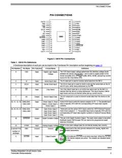
Figure 3. 33810 Pin Connections
Table 1. 33810 Pin Definitions
A functional description of each pin can be found in the Functional Pin Description section beginning on page 13.
Pin Number Pin Name Pin Function
Formal Name
Definition
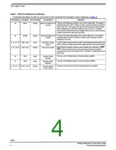
The VDD input supply voltage determines the interface voltage levels
between the device and the MCU, and is used to supply power to the
Serial Out buffer (SO), SPKDUR buffer, MAXI, NOMI, and pull-up current
source for the Chip Select (CS).
8
VDD
Input
Digital Logic Supply
Voltage
The SI input pin is used to receive serial data from the MCU.
6
5
SI
Input
Input
Serial Input Data
Serial Clock Input
The SCLK input pin is used to clock in and out the serial data on the SI
and SO pins, while being addressed by the CS.
SCLK
The Chip Select input pin is an active low signal sent by the MCU to
indicate that the device is being addressed. This input requires CMOS
logic levels and has an internal active pull-up current source.
4
7
CS
SO
Input
Chip Select
The SO output pin is used to transmit serial data from the device to the
MCU.
Output
Input
Serial Output Data
Active HIGH input control for injector outputs OUT0 - 3. The parallel input
data is logically OR’d with the corresponding SPI input data register
contents.
10, 11, 12, 13 DIN0,DIN1,
DIN2,DIN3
Driver Input 0, Driver
Input 1, Driver Input 2,
Driver Input 3
These pins are the active HIGH input control for IGBT/General Purpose
Gate Driver outputs 0 - 3. The parallel input data is logically OR'd with the
corresponding SPI input data register contents in General Purpose Mode
Only.
24, 23, 22, 21 GIN0,GIN1,
GIN2,GIN3
Input
Gate Driver Input 0
Gate Driver Input 1
Gate Driver Input 2
Gate Driver Input 3
This pin is the Spark Duration Output. This open drain output is low while
feedback inputs FB0 through FB3 are above the programmed spark
detection threshold.
20
SPKDUR
Output
Spark Duration Output
VPWR is the main voltage input for all internal analog bias circuitry.
25
VPWR
GND
Input
Analog Supply Voltage
Ground
This exposed pad is the only ground reference for analog, digital and
power ground connections.
Exposed Pad
Ground
(bottom of
package)
The Output Enable pin (OUTEN) is an active low input. When the OUTEN
pin is low, the device outputs are active. The outputs are disabled when
OUTEN is high.
9
OUTEN
Input
Output Enable
33810
Analog Integrated Circuit Device Data
Freescale Semiconductor
3

 FREESCALE [ Freescale ]