Freescale Semiconductor, Inc.
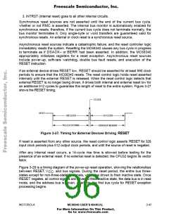
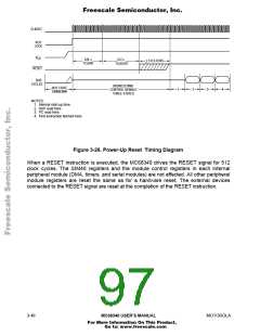
CLKOUT
VCO
LOCK
V
CC
328 ×
TCLKIN
×
512
14 CLOCKS
≤
TCLKOUT
RESET
BUS
CYCLES
ADDRESS AND
CONTROL SIGNALS
THREE-STATED
BUS STATE
UNKNOWN
1
2
3
4
NOTES:
1. Internal start-up time.
2. SSP read here.
3. PC read here.
4. First instruction fetched here.
Figure 3-28. Power-Up Reset Timing Diagram
When a RESET instruction is executed, the MC68340 drives the RESET signal for 512
clock cycles. The SIM40 registers and the module control registers in each internal
peripheral module (DMA, timers, and serial modules) are not affected. All other peripheral
module registers are reset the same as for a hardware reset. The external devices
connected to the RESET signal are reset at the completion of the RESET instruction.
3- 48
MC68340 USER’S MANUAL
MOTOROLA
For More Information On This Product,
Go to: www.freescale.com

 FREESCALE [ Freescale ]