Freescale Semiconductor, Inc.
The external bus interface (EBI) handles the transfer of information between the internal
CPU32 and memory, peripherals, or other processing elements in the external address
space. See Section 3 Bus Operation for further information.
The MC68340 dynamically interprets the port size of an addressed device during each
bus cycle, allowing operand transfers to or from 8-, 16-, and 32-bit ports. The device
signals its port size and indicates completion of the bus cycle through the use of the
DSACK≈ inputs. Dynamic bus sizing allows a programmer to write code that is not bus-
width specific. For a discussion on dynamic bus sizing, see Section 3 Bus Operation.
The MC68340 includes dedicated user-accessible test logic that is fully compliant with the
IEEE 1149.1 Standard Test Access Port and Boundary Scan Architecture. Problems
associated with testing high-density circuit boards have led to the development of this
standard under the sponsorship of the IEEE Test Technology Committee and Joint Test
Action Group (JTAG). The MC68340 implementation supports circuit-board test strategies
based on this standard. Refer to Section 9 IEEE 1149.1 Test Access Port for additional
information.
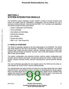
4.2 MODULE OPERATION
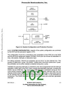
The following paragraphs describe the operation of the module base address register,
system configuration and protection, clock synthesizer, chip select functions, and the
external bus interface.
NOTE
The terms assert and negate are used throughout this section
to avoid confusion when dealing with a mixture of active-low
and active-high signals. The term assert or assertion indicates
that a signal is active or true independent of the level
represented by a high or low voltage. The term negate or
negation indicates that a signal is inactive or false.
4.2.1 Module Base Address Register Operation
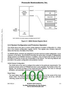
The module base address register (MBAR) controls the location of all internal module
registers (see 4.3.1 Module Base Address Register (MBAR)). The address stored in this
register is the base address (starting location) for all internal registers. All internal module
registers are contained in a single 4-Kbyte block (see Figure 4-1) that is relocatable along
4-Kbyte boundaries.
The location of the internal registers is fixed by writing the desired base address of the
4-Kbyte block to the MBAR using the MOVES instruction to address $0003FF00 in CPU
space. The source function code (SFC) and destination function code (DFC) registers
contain the address space values (FC3–FC0) for the read or write operand of the MOVES
instruction (see Section 5 CPU32 or M68000PM/AD, Programmer’s Reference Manual).
Therefore, the SFC or DFC register must indicate CPU space (FC3–FC0 = $7), using the
MOVEC instruction, before accessing MBAR. The offset from the base address is shown
above each register diagram.
4- 2
MC68340 USER’S MANUAL
MOTOROLA
For More Information On This Product,
Go to: www.freescale.com

 FREESCALE [ Freescale ]