Freescale Semiconductor, Inc.
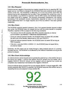
3.6.4 Bus Arbitration Control
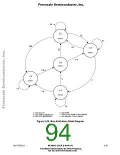
The bus arbitration control unit in the MC68340 is implemented with a finite state machine.
As discussed previously, all asynchronous inputs to the MC68340 are internally
synchronized in a maximum of two cycles of the clock. As shown in Figure 3-25 input
signals labeled R and A are internally synchronized versions of BR and BGACK
respectively. The BG output is labeled G, and the internal high-impedance control signal is
labeled T. If T is true, the address, data, and control buses are placed in the high-
impedance state after the next rising edge following the negation of AS and RMC. All
signals are shown in positive logic (active high) regardless of their true active voltage
level. The state machine shown in Figure 3-25 does not have a state 1 or state 4.
State changes occur on the next rising edge of the clock after the internal signal is valid.
The BG signal transitions on the falling edge of the clock after a state is reached during
which G changes. The bus control signals (controlled by T) are driven by the MC68340
immediately following a state change, when bus mastership is returned to the MC68340.
State 0, in which G and T are both negated, is the state of the bus arbiter while the
MC68340 is bus master. R and A keep the arbiter in state 0 as long as they are both
negated.
The MC68340 does not allow arbitration of the external bus during the RMC sequence.
For the duration of this sequence, the MC68340 ignores the BR input. If mastership of the
bus is required during an RMC operation, BERR must be used to abort the RMC sequence.
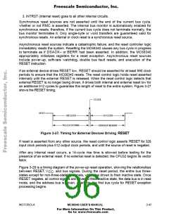
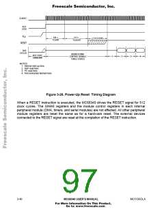
3.6.5 Show Cycles
The MC68340 can perform data transfers with its internal modules without using the
external bus, but, when debugging, it is desirable to have address and data information
appear on the external bus. These external bus cycles, called show cycles, are
distinguished by the fact that AS is not asserted externally. DS is used to signal address
strobe timing in show cycles.
After reset, show cycles are disabled and must be enabled by writing to the SHEN bits in
the module configuration register (see 4.3.2.1 Module Configuration Register (MCR)).
When show cycles are disabled, the A31–A0, FCx, SIZx, and R/W signals continue to
reflect internal bus activity. However, AS and DS are not asserted externally, and the
external data bus remains in a high-impedance state. When show cycles are enabled, DS
indicates address strobe timing and the external data bus contains data. The following
paragraphs are a state-by-state description of show cycles, and Figure 3-26 illustrates a
show cycle timing diagram. Refer to Section 11 Electrical Characteristics for specific
timing information.
3- 44
MC68340 USER’S MANUAL
MOTOROLA
For More Information On This Product,
Go to: www.freescale.com

 FREESCALE [ Freescale ]