Freescale Semiconductor, Inc.
SECTION 4
SYSTEM INTEGRATION MODULE
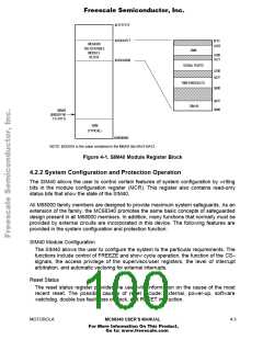
The MC68340 system integration module (SIM40) consists of several functions that
control the system start-up, initialization, configuration, and the external bus with a
minimum of external devices. It also provides the IEEE 1149.1 boundary scan capabilities.
The SIM40 includes the following functions:
• System Configuration and Protection
• Clock Synthesizer
• Chip Selects and Wait States
• External Bus Interface
• Bus Arbitration
• Dynamic Bus Sizing
• IEEE 1149.1 Test Access Port
4.1 MODULE OVERVIEW
The SIM40 is essentially identical to the SIM implemented in the MC68330. The SIM40
has similar features to the SIM in the MC68331, MC68332, and MC68333. The periodic
interrupt timer, double bus fault monitor, software watchdog, internal bus monitor, and
spurious interrupt monitor are identical. However, many of the other features in the SIM's
differ in their use and details.
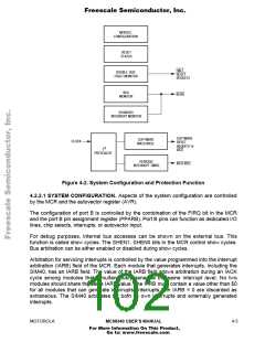
The system configuration and protection function controls system configuration and
provides various monitors and timers, including the internal bus monitor, double bus fault
monitor, spurious interrupt monitor, software watchdog timer, and the periodic interrupt
timer.
The clock synthesizer generates the clock signals used by the SIM40 and the other on-
chip modules, as well as CLKOUT used by external devices.
The programmable chip select function provides four chip select signals that can enable
external memory and peripheral circuits, providing all handshaking and timing signals.
Each chip select signal has an associated base address register and an address mask
register that contain the programmable characteristics of that chip select. Up to three wait
states can be programmed by setting bits in the address mask register.
MOTOROLA
MC68340 USER’S MANUAL
4- 1
For More Information On This Product,
Go to: www.freescale.com

 FREESCALE [ Freescale ]