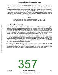
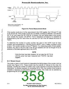
Freescale Semiconductor, Inc.
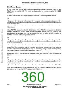
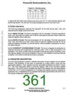
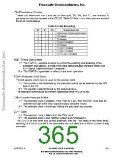
Table 8-1. OCx Encoding
OC1
OC0
TOUTx
0
0
1
1
0
1
0
1
Hi-Z
0
0
1
A read of the SR while in this mode always shows the TO, TC, and COM bits cleared, and
the PO bits as $FF. The SR OUT bit always indicates the level on the TOUTx pin.
8.3.9 Bus Operation
The following paragraphs describe the operation of the IMB during read, write, and
interrupt acknowledge cycles to the timer.
8.3.9.1 READ CYCLES. The timer is accessed with no wait states. The timer responds to
byte, word, and long-word reads, and 16 bits of valid data are returned. Read cycles from
reserved registers return logic zero.
8.3.9.2 WRITE CYCLES. The timer is accessed with no wait states. The timer responds to
byte, word, and long-word writes. Write cycles to read-only registers and bits as well as
reserved registers complete in a normal manner without exception processing; however,
the data is ignored.
8.3.9.3 INTERRUPT ACKNOWLEDGE CYCLES. The timer is capable of arbitrating for
interrupt servicing and supplying the interrupt vector when it has successfully won
arbitration. The vector number must be provided if interrupt servicing is necessary; thus,
the interrupt register (IR) must be initialized. If the IR is not initialized, a spurious interrupt
exception will be taken if interrupt servicing is necessary.
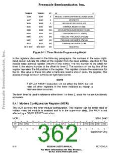
8.4 REGISTER DESCRIPTION
The following paragraphs contain a detailed description of each register and its specific
function. The operation of the timer is controlled by writing control words into the
appropriate registers. Timer registers and their associated addresses are listed in Figure
8-11. For more information about a particular register, refer to the individual register
description. The ADDR column indicates the offset of the register from the base address
of the timer. An FC column designation of S indicates that register access is restricted to
supervisor only. A designation of S/U indicates that access is governed by the SUPV bit in
the module configuration register (MCR).
MOTOROLA
MC68340 USER’S MANUAL
8- 17
For More Information On This Product,
Go to: www.freescale.com

 FREESCALE [ Freescale ]