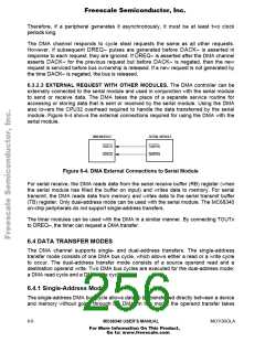
Freescale Semiconductor, Inc.
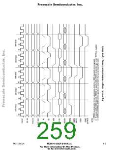
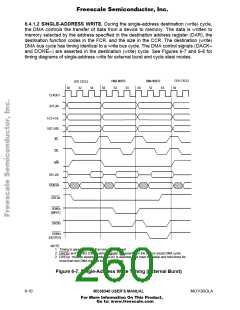
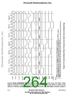
6.4.1.2 SINGLE-ADDRESS WRITE. During the single-address destination (write) cycle,
the DMA controls the transfer of data from a device to memory. The data is written to
memory selected by the address specified in the destination address register (DAR), the
destination function codes in the FCR, and the size in the CCR. The destination (write)
DMA bus cycle has timing identical to a write bus cycle. The DMA control signals (DACK≈
and DONE≈) are asserted in the destination (write) cycle. See Figures 6-7 and 6-8 for
timing diagrams of single-address write for external burst and cycle steal modes.
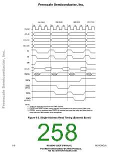
CPU CYCLE
S0
DMA WRITE
S2 S4
DMA WRITE
S2 S4
CPU CYCLE
S2
S0
S4
S0
S0
CLKOUT
A31–A0
FC3–FC0
SIZ1-SIZ0
AS
DS
R/W
D15–D0
DSACKx
DREQx
DONEx
.
DONEx
(OUTPUT)
NOTE:
1. Timing to generate more than one DMA request.
2. DACKx and DONEx (DMA control signals) are asserted in the source (read) DMA cycle.
2. DREQx must be asserted while DACKx is asserted, and meet the setup and hold times for
more than one DMA transfer to be recognized.
Figure 6-7. Single-Address Write Timing (External Burst)
6- 10
MC68340 USER’S MANUAL
MOTOROLA
For More Information On This Product,
Go to: www.freescale.com

 FREESCALE [ Freescale ]