Freescale Semiconductor, Inc.
Electrical Specifications
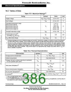
Tables of Data
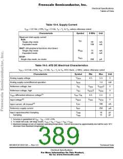
Table 19-4. Supply Current
V
DD = 5.0 Vdc ±10%, VSS = 0 Vdc, TA = TL to TH, unless otherwise noted
Characteristic
Symbol
8 MHz
Unit
Maximum total supply current
RUN:
IDD
Single-chip mode
Expanded mode
60
100
mA
mA
WAIT: (All peripheral functions shut down)
Single-chip mode
WIDD
15
20
mA
mA
Expanded mode
STOP:
SIDD
Single-chip mode, no clocks
200
µA
Table 19-5. ATD DC Electrical Characteristics
V
DD = 5.0 Vdc ±10%, VSS = 0 Vdc, TA = TL to TH, ATD Clock = 2 MHz, unless otherwise noted
Characteristic
Symbol
Min
Max
5.5
Unit
V
VDDA
Analog supply voltage
4.5
IDDA
VRL
VRH
Analog supply currentNormal operation
Reference voltage, low
1.0
mA
V
VSSA
V
DDA/2
VDDA/2
VDDA
Reference voltage, high
V
REF differential reference voltage(1)
V
RH−VRL
VINDC
IOFF
4.5
5.5
VDDA
100
V
V
V
Input voltage(2)
VSSA
Input current, off channel(3)
Reference supply current
nA
µA
IREF
250
CINN
CINS
Input capacitanceNot Sampling
Sampling
10
15
pF
pF
1. Accuracy is guaranteed at VRH − VRL = 5.0V ±10%.
2. To obtain full-scale, full-range results, VSSA ≤ VRL ≤ VINDC ≤ VRH ≤ VDDA
.
3. Maximum leakage occurs at maximum operating temperature. Current decreases by approximately one-half for each 10°C
decrease from maximum temperature.
MC68HC912DG128 — Rev 3.0
Technical Data
Electrical Specifications
For More Information On This Product,
Go to: www.freescale.com

 FREESCALE [ Freescale ]