Freescale Semiconductor, Inc.
Electrical Specifications
19.3 Tables of Data
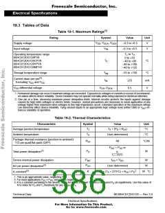
Table 19-1. Maximum Ratings(1)
Rating
Symbol
VDD, VDDA, VDDX
VIN
Value
Unit
V
Supply voltage
Input voltage
−0.3 to +6.5
−0.3 to +6.5
TL to TH
V
Operating temperature range
68HC912DG128PV8
68HC912DG128CPV8
68HC912DG128VPV8
68HC912DG128MPV8
0 to +70
TA
°C
−40 to +85
−40 to +105
−40 to +125
Tstg
IIN
DD−VDDX
Storage temperature range
−55 to +150
±25
°C
mA
V
Current drain per pin(2)
Excluding VDD and VSS
VDD differential voltage
V
6.5
1. Permanent damage can occur if maximum ratings are exceeded. Exposures to voltages or currents in excess of recommend-
ed values affects device reliability. Device modules may not operate normally while being exposed to electrical extremes.
2. One pin at a time, observing maximum power dissipation limits. Internal circuitry protects the inputs against damage
caused by high static voltages or electric fields; however, normal precautions are necessary to avoid application of any
voltage higher than maximum-rated voltages to this high-impedance circuit. Extended operation at the maximum ratings
can adversely affect device reliability. Tying unused inputs to an appropriate logic voltage level (either GND or VDD) en-
hances reliability of operation.
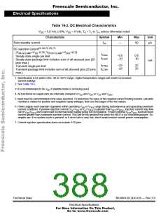
Table 19-2. Thermal Characteristics
Characteristic
Average junction temperature
Symbol
Value
Unit
°C
TJ
TA + (PD × ΘJA)
TA
Ambient temperature
User-determined
40
°C
Package thermal resistance (junction-to-ambient)
112-pin quad flat pack (QFP)
ΘJA
°C/W
PINT + PI/O or
Total power dissipation(1)
PD
W
K
-------------------------
TJ + 273°C
PINT
PI/O
IDD × VDD
Device internal power dissipation
I/O pin power dissipation(2)
A constant(3)
W
W
User-determined
2
K
W · °C
PD × (TA + 273°C) + ΘJA × PD
1. This is an approximate value, neglecting PI/O
.
2. For most applications PI/O « PINT and can be neglected.
3. K is a constant pertaining to the device. Solve for K with a known TA and a measured PD (at equilibrium). Use this value of
K to solve for PD and TJ iteratively for any value of TA.
Technical Data
MC68HC912DG128 — Rev 3.0
Electrical Specifications
For More Information On This Product,
Go to: www.freescale.com

 FREESCALE [ Freescale ]