Freescale Semiconductor, Inc.
Electrical Specifications
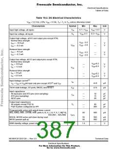
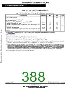
Table 19-3. DC Electrical Characteristics
V
DD = 5.0 Vdc ±10%, VSS = 0 Vdc, TA = TL to TH, unless otherwise noted
Characteristic
Symbol
Min
Max
Unit
Isb
Ram standby current
—
50
µA
DC injection current(3) (4) (5) (6) (7)
(VNEGCLAMP=VSS–0.3V, VPOSTCLAMP=VDDE+0.3)
Steady state single pin limit
Steady state package limit includes sum of all stressed pins (25
IICsss
IICssP
–0.5
–10
0.5
10
mA
pins max.)
Transient single pin limit
Transient package limit includes sum of all stressed pins (25 pins
max.)
IICTRs
IICTRP
–25
–25
25
25
1. Specification is for parts in the -40 to +85°C range. Higher temperature ranges will result in increased
current leakage.
2. See Table 19-5.
3. It is recommended to tie VDD if standby mode is not being used.
4. All functional no-supply pins are internally clamped to VSS and VDD or VSS and VDDX
.
5. Input must be current limited to the value specified. To determine the value of the required current-limiting resistor, calculate
resistance values for positive and negative clamp voltages, then use the larger of the two values.
6. Power supply must maintain regulation within operating VDD or VDDX range during instantaneous and operating maximum
current conditions. If positive injection current (Vin>VDD or Vin>VDDX) is greater than IDD or IDDX, injection current may flow
out of VDD/VDDX and could result in external power supply going out of regulation. Ensure external VDD/VDDX load will shunt
current greater than maximum injection current. This will be the greatest risk when the MCU is not consuming power. Ex-
amples are: if no system clock is present, or if clock rate is very low, which would reduce overall power consumption.
7. Current injection specification does not include ATD pins.
Technical Data
MC68HC912DG128 — Rev 3.0
Electrical Specifications
For More Information On This Product,
Go to: www.freescale.com

 FREESCALE [ Freescale ]