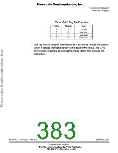
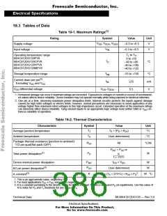
Freescale Semiconductor, Inc.
Electrical Specifications
Tables of Data
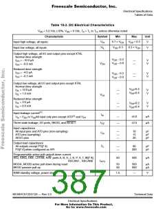
Table 19-3. DC Electrical Characteristics
V
DD = 5.0 Vdc ±10%, VSS = 0 Vdc, TA = TL to TH, unless otherwise noted
Characteristic
Symbol
Min
Max
Unit
V
VIH
0.7 × VDD
V
DD + 0.3
Input high voltage, all inputs
Input low voltage, all inputs
VIL
V
SS−0.3
0.2 × VDD
V
Output high voltage, all I/O and output pins except XTAL
Normal drive strength
V
V
DD − 0.2
DD − 0.8
IOH = −10.0 µA
—
—
V
V
VOH
IOH = −0.8 mA
Reduced drive strength
I
OH = −4.0 µA
V
V
DD − 0.2
DD − 0.8
—
—
V
V
IOH = −0.3 mA
Output low voltage, all I/O and output pins except XTAL
Normal drive strength
V
SS+0.2
SS+0.4
IOL = 10.0 µA
—
—
V
V
V
IOL = 1.6 mA
VOL
Reduced drive strength
I
OL = 3.6 µA
—
—
V
SS+0.2
SS+0.4
V
V
IOL = 0.6 mA
V
Input leakage current(1)
Vin = VDD or VSSAll input only pins except ATD(2) and VFP
Iin
—
—
±5.0
±2.5
µA
µA
IOZ
Three-state leakage, I/O ports, BKGD, and RESET
Input capacitance
All input pins and ATD pins (non-sampling)
ATD pins (sampling)
All I/O pins
—
—
—
10
15
20
pF
pF
pF
Cin
Output load capacitance
All outputs except PS[7:4]
PS[7:4] when configured as SPI
CL
—
—
90
200
pF
pF
Programmable active pull-up/pull-down current
IRQ, XIRQ, DBE, LSTRB, R/W. ports A, B, H, J, K, P, S, T, IB[7:4],
RXCAN1, .RXCAN0
50
500
µA
IAPU
MODA, MODB active pull down during reset
BKGD passive pull up
50
50
500
500
µA
µA
Vsb
RAM standby voltage, power down
1.5
—
V
MC68HC912DG128 — Rev 3.0
Electrical Specifications
Technical Data
For More Information On This Product,
Go to: www.freescale.com

 FREESCALE [ Freescale ]