Freescale Semiconductor, Inc.
Inter-IC Bus
IIC Register Descriptions
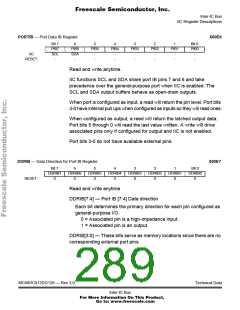
PORTIB — Port Data IB Register
$00E6
Bit 7
PIB7
SCL
-
6
PIB6
SDA
-
5
4
3
2
1
Bit 0
PIB5
PIB4
PIB3
PIB2
PIB1
PIB0
IIC
-
-
-
-
-
-
-
-
-
-
-
-
RESET:
Read and write anytime.
IIC functions SCL and SDA share port IB pins 7 and 6 and take
precedence over the general-purpose port when IIC is enabled. The
SCL and SDA output buffers behave as open-drain outputs.
When port is configured as input, a read will return the pin level. Port bits
3-0 have internal pull ups when configured as inputs so they will read ones.
When configured as output, a read will return the latched output data.
Port bits 5 through 0 will read the last value written. A write will drive
associated pins only if configured for output and IIC is not enabled.
Port bits 3-0 do not have available external pins.
DDRIB — Data Direction for Port IB Register
$00E7
Bit 7
DDRIB7
0
6
DDRIB6
0
5
DDRIB5
0
4
DDRIB4
0
3
DDRIB3
0
2
DDRIB2
0
1
DDRIB1
0
Bit 0
DDRIB0
0
RESET:
Read and write anytime
DDRIB[7:4] — Port IB [7:4] Data direction
Each bit determines the primary direction for each pin configured as
general-purpose I/O.
0 = Associated pin is a high-impedance input.
1 = Associated pin is an output.
DDRIB[3:0] — These bits serve as memory locations since there are no
corresponding external port pins.
MC68HC912DG128 — Rev 3.0
Technical Data
Inter-IC Bus
For More Information On This Product,
Go to: www.freescale.com

 FREESCALE [ Freescale ]