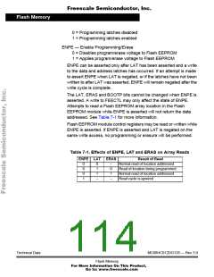
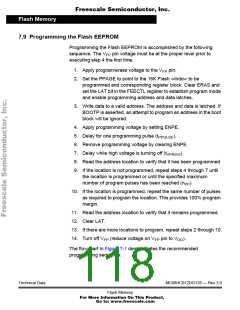
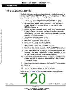
Freescale Semiconductor, Inc.
Flash Memory
valid address to the array after LAT is set will cause the address and
data to be latched into the programming latches. Once the address and
data are latched, write accesses to the array will be ignored while LAT is
set. Writes to the control registers will occur normally.
Program/Erase Verification — When programming or erasing the
Flash EEPROM array, a special verification method is required to ensure
that the program/erase process is reliable, and also to provide the
longest possible life expectancy. This method requires stopping the
program/erase sequence at periods of tPPULSE (tEPULSE for erasing) to
determine if the Flash EEPROM is programmed/erased. After the
location reaches the proper value, it must continue to be
programmed/erased with additional margin pulses to ensure that it will
remain programmed/erased. Failure to provide the margin pulses could
lead to corrupted or unreliable data.
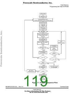
Program/Erase Sequence — To begin a program or erase sequence
the external VFP voltage must be applied and stabilized. The ERAS bit
must be set or cleared, depending on whether a program sequence or
an erase sequence is to occur. The LAT bit will be set to cause any
subsequent data written to a valid address within the Flash EEPROM to
be latched into the programming address and data latches. The next
Flash array write cycle must be either to the location that is to be
programmed if a programming sequence is being performed, or, if
erasing, to any valid Flash EEPROM array location. Writing the new
address and data information to the Flash EEPROM is followed by
assertion of ENPE to turn on the program/erase voltage to
program/erase the new location(s). The LAT bit must be asserted and
the address and data latched to allow the setting of the ENPE control bit.
If the data and address have not been latched, an attempt to assert
ENPE will be ignored and ENPE will remain negated after the write cycle
to FEECTL is completed. The LAT bit must remain asserted and the
ERAS bit must remain in its current state as long as ENPE is asserted.
A write to the LAT bit to clear it while ENPE is set will be ignored. That
is, after the write cycle, LAT will remain asserted. Likewise, an attempt
to change the state of ERAS will be ignored and the state of the ERAS
bit will remain unchanged.
Technical Data
MC68HC912DG128 — Rev 3.0
Flash Memory
For More Information On This Product,
Go to: www.freescale.com

 FREESCALE [ Freescale ]