Freescale Semiconductor, Inc.
Flash Memory
0 = Programming latches disabled
1 = Programming latches enabled
ENPE — Enable Programming/Erase
0 = Disables program/erase voltage to Flash EEPROM
1 = Applies program/erase voltage to Flash EEPROM
ENPE can be asserted only after LAT has been asserted and a write
to the data and address latches has occurred. If an attempt is made
to assert ENPE when LAT is negated, or if the latches have not been
written to after LAT was asserted, ENPE will remain negated after the
write cycle is complete.
The LAT, ERAS and BOOTP bits cannot be changed when ENPE is
asserted. A write to FEECTL may only affect the state of ENPE.
Attempts to read a Flash EEPROM array location in the Flash
EEPROM module while ENPE is asserted will not return the data
addressed. See Table 7-1 for more information.
Flash EEPROM module control registers may be read or written while
ENPE is asserted. If ENPE is asserted and LAT is negated on the
same write access, no programming or erasure will be performed.
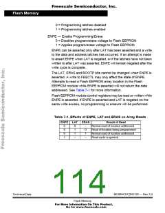
Table 7-1. Effects of ENPE, LAT and ERAS on Array Reads
ENPE LAT
ERAS
Result of Read
0
0
0
1
0
1
1
–
–
0
1
–
Normal read of location addressed
Read of location being programmed
Normal read of location addressed
Read cycle is ignored
Technical Data
MC68HC912DG128 — Rev 3.0
Flash Memory
For More Information On This Product,
Go to: www.freescale.com

 FREESCALE [ Freescale ]