Freescale Semiconductor, Inc.
Flash Memory
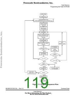
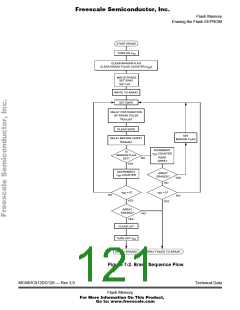
7.9 Programming the Flash EEPROM
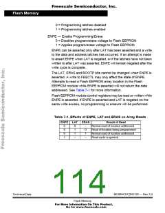
Programming the Flash EEPROM is accomplished by the following
sequence. The VFP pin voltage must be at the proper level prior to
executing step 4 the first time.
1. Apply program/erase voltage to the VFP pin.
2. Set the PPAGE to point to the 16K Flash window to be
programmed and corresponding register block. Clear ERAS and
set the LAT bit in the FEECTL register to establish program mode
and enable programming address and data latches.
3. Write data to a valid address. The address and data is latched. If
BOOTP is asserted, an attempt to program an address in the boot
block will be ignored.
4. Apply programming voltage by setting ENPE.
5. Delay for one programming pulse (tPPULSE).
6. Remove programming voltage by clearing ENPE.
7. Delay while high voltage is turning off (tVPROG).
8. Read the address location to verify that it has been programmed
9. If the location is not programmed, repeat steps 4 through 7 until
the location is programmed or until the specified maximum
number of program pulses has been reached (nPP)
10. If the location is programmed, repeat the same number of pulses
as required to program the location. This provides 100% program
margin.
11. Read the address location to verify that it remains programmed.
12. Clear LAT.
13. If there are more locations to program, repeat steps 2 through 10.
14. Turn off VFP (reduce voltage on VFP pin to VDD).
The flowchart in Figure 7-1 demonstrates the recommended
programming sequence.
Technical Data
MC68HC912DG128 — Rev 3.0
Flash Memory
For More Information On This Product,
Go to: www.freescale.com

 FREESCALE [ Freescale ]