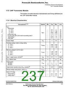
Freescale Semiconductor, Inc.
Preliminary Electrical Specifications
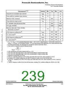
UHF Transmitter Module
(1) (2)
Symbol
Min
10
Typ
—
Max
—
Unit
µs
Characteristic
t
Setup time for modulation type selection
Pulse width for modulation type selection
Maximum XTAL resistance
SMD
t
10
—
—
µs
WD
R
—
200
—
W
XTAL
I
Phase detector output current
PLL bandwith using internal loop filter
VCO gain, 434 MHz
—
—
—
10
—
—
—
µA
kHz
Out
—
—
280
1000
MHz/V
Maximum data rate in FSK, 434 MHz
—
9.6
—
—
kBd
(7)
Manchester encoded
(8)
t
—
—
—
—
200
50
500
500
500
750
µs
µs
µs
µs
µPclk frequency settling time
supck
(9)
t
PLL lock in time
spl
(10)
t
200
250
µPclk frequency settling time
supck1
(11)
t
PLL lock-in time
spll1
1. VCC = 3 V, REXT = 12 K, operating temperature range = –40°C to 85°C, output frequency = 433.92 MHz, reference fre-
quency = 13.56 MHz, UPCLK frequency divider = 16, OOK mode selected, and output load is 50 Ω, unless otherwise noted
2. For timing measurements, the data input rise and fall times must be lower than 100 ns.
3. Peak current is calculated using the following formula:
P
dBm
20
---------------- – 1. 5
10
I
= -----------------------------
Peak
5
4. 0 dB corresponds to the power obtained with REXT=12 K
5. From 50% of the data rising edge to 50% of the corresponding RF signal envelope edge
6. From 50% of the data falling edge to 50% of the corresponding RF signal envelope edge
7. Depends on external fiter on PFD pin
8. From 0 to 1 transition at MODE to UPCLK duty cycle better than 55/45 XTAL series resistance at 150 Ω
9. Excluding XTAL oscillator settling time and until RF frequency is within 30 kHz from the final value
10. From 0 to 1 transition at PLLEN to UPCLK duty cycle, better than 55/45 XTAL series resistance at 150 Ω , mode set
to GND
11. Until RF frequency is within 30 kHz from the final value, including XTAL oscillator settling time, MODE set to GND
MC68HC908RFRK2
MOTOROLA
AdvanceInformation
239
Preliminary Electrical Specifications
For More Information On This Product,
Go to: www.freescale.com

 FREESCALE [ Freescale ]