Freescale Semiconductor, Inc.
Preliminary Electrical Specifications
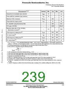
Memory Characteristics
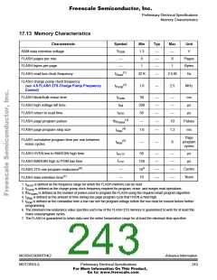
17.13 Memory Characteristics
Characteristic
RAM data retention voltage
FLASH pages per row
Symbol
Min
1.3
8
Typ
—
Max
—
8
Unit
V
V
RDR
—
—
(1)
—
Pages
Bytes
FLASH bytes per page
1
—
1
FLASH read bus clock frequency
32 K
—
2.5 M
Hz
f
Read
FLASH charge pump clock frequency
(see 4.5 FLASH 2TS Charge Pump Frequency
Control)
(2)
1.8
—
2.5
MHz
f
Pump
t
FLASH block/bulk erase time
FLASH high voltage kill time
FLASH return to read time
FLASH page program pulses
30
200
50
—
—
—
—
—
—
—
10
ms
µs
Erase
t
Kill
t
µs
HVD
(3)
—
Pulses
fls
t
Pulses
(4)
FLASH page program step size
1.0
—
—
—
1.2
8
ms
Step
Row
Page
program
cycles
FLASH cumulative program time per row between
erase cycles
(5)
t
t
FLASH HVEN low to MARGIN high time
FLASH MARGIN high to PGM low time
50
—
—
—
—
µs
µs
HVTV
t
150
VTP
(6)
4
—
—
-—
-—
-—
-—
Cycles
Years
FLASH 2TS row program endurance
10
(7)
10
FLASH data retention time
1. fREAD is defined as the frequency range for which the FLASH memory can be read.
2. f is defined as the charge pump clock frequency required for program, erase, and margin read operations.
Pump
3. fls
is defined as the number of pulses used to program the FLASH using the required smart program algorithm.
Pulses
4. t
5. t
is defined as the amount of time during one page program cycle that HVEN is held high.
is defined as the cumulative time a row can see the program voltage before the row must be erased before further
Step
Row
programming.
6. The minimum row endurance value specifies each row of the FLASH 2TS memory is guaranteed to work for at least this
many erase/program cycles.
7. The FLASH is guaranteed to retain data over the entire temperature range for at least the minimum time specified.
MC68HC908RFRK2
MOTOROLA
AdvanceInformation
243
Preliminary Electrical Specifications
For More Information On This Product,
Go to: www.freescale.com

 FREESCALE [ Freescale ]