Freescale Semiconductor, Inc.
Preliminary Electrical Specifications
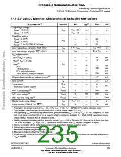
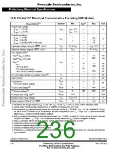
17.8 2.0-Volt DC Electrical Characteristics Excluding UHF Module
(1)
(2)
Symbol
Min
Max
Unit
Characteristic
Output high voltage
Typ
(I
= –1.2 mA)
V
V
–0.3
V
—
—
—
—
V
Load
Load
DD
DD
OH
(I
= –2.0 mA)
–1.0
Output low voltage
(I
(I
(I
= 1.2 mA)
Load
Load
Load
—
—
—
—
—
—
0.3
1.0
0.3
V
V
OL
= 3.0 mA)
= 3.0 mA) PTA7–PTA0 only
V
0.7 x V
V
+ 0.3
DD
Input high voltage, all ports, IRQ1, OSC1
Input low voltage, all ports, IRQ1, OSC1
—
—
V
V
IH
DD
V
V
0.3 x V
DD
IL
SS
V
supply current
DD
(3)
—
—
—
—
2.5
850
mA
mA
Run (f = 2.0 MHz)
op
(4)
Wait (f = 2.0 MHz)
op
(5)
I
Stop
DD
—
—
—
—
10
—
50
—
—
100
—
nA
nA
µA
µA
25°C
–40 °C to 85°C
25°C with LVI enabled
–40°C to 85°C with LVI enabled
350
(6)
I
—
—
—
—
± 1
± 1
µA
µA
I/O ports high-impedance leakage current
Input current
IL
I
In
C
Capacitance
—
—
—
—
12
8
Out
pF
Ports (as input or output)
C
In
(7)
V
0
0
—
700
—
200
800
—
mV
mV
V/ms
V
POR re-arm voltage
POR
POR
POR
(8)
V
R
POR reset voltage
(9)
0.02
POR rise time ramp rate
V
V
+ 2.5
DD
Monitor mode entry voltage
—
8
HI
R
Pullup resistor, PTA6–PTA1, IRQ1
70
—
120
kΩ
PU
1. Parameters are design targets at VDD = 2.0 ± 10%, VSS = 0 Vdc, TA = –40oC to +85oC, unless otherwise noted
2. Typical values reflect average measurements at midpoint of voltage range, 25°C only.
3. Run (operating) IDD measured using internal clock generator module (fop= 2.0 MHz). VDD = 2.0 Vdc. All inputs 0.2 V from
rail. No dc loads. Less than 100 pF on all outputs. All ports configured as inputs. CL = 20 pF. OSC2 capacitance linearly
affects run IDD. Measured with all modules enabled.
4. Wait IDD measured using internal clock generator module, fOP = 2.0 MHz. All inputs 0.2 V from rail; no dc loads; less than
100 pF on all outputs. CL = 20 pF. OSC2 capacitance linearly affects wait IDD. All ports configured as inputs.
5. Stop IDD measured with no port pins sourcing current, all modules disabled except as noted.
6. Pullups and pulldowns are disabled.
7. Maximum is highest voltage that POR is guaranteed.
8. Maximum is highest voltage that POR is possible.
9. If minimum VDD is not reached before the internal POR reset is released, RST must be driven low externally until minimum
VDD is reached.
Advance Information
236
MC68HC908RFRK2
MOTOROLA
Preliminary Electrical Specifications
For More Information On This Product,
Go to: www.freescale.com

 FREESCALE [ Freescale ]