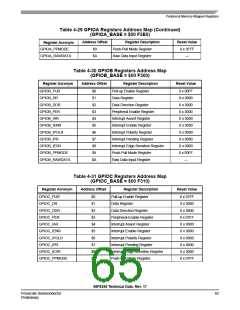
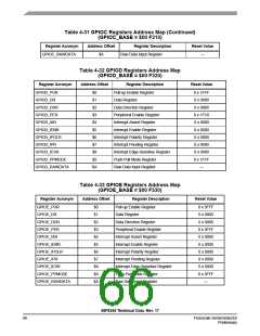
Table 4-31 GPIOC Registers Address Map (Continued)
(GPIOC_BASE = $00 F310)
Register Acronym
Address Offset
Register Description
Reset Value
GPIOC_RAWDATA
$A
Raw Data Input Register
—
Table 4-32 GPIOD Registers Address Map
(GPIOD_BASE = $00 F320)
Register Acronym
Address Offset
Register Description
Pull-up Enable Register
Reset Value
GPIOD_PUR
GPIOD_DR
$0
$1
$2
$3
$4
$5
$6
$7
$8
$9
$A
0 x 1FFF
0 x 0000
0 x 0000
0 x 1FC0
0 x 0000
0 x 0000
0 x 0000
0 x 0000
0 x 0000
0 x 1FFF
—
Data Register
GPIOD_DDR
GPIOD_PER
GPIOD_IAR
Data Direction Register
Peripheral Enable Register
Interrupt Assert Register
Interrupt Enable Register
Interrupt Polarity Register
Interrupt Pending Register
Interrupt Edge-Sensitive Register
Push-Pull Mode Register
Raw Data Input Register
GPIOD_IENR
GPIOD_IPOLR
GPIOD_IPR
GPIOD_IESR
GPIOD_PPMODE
GPIOD_RAWDATA
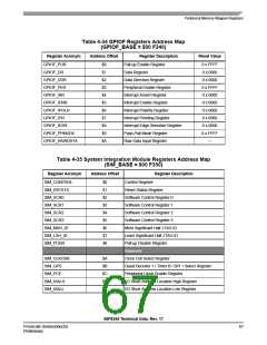
Table 4-33 GPIOE Registers Address Map
(GPIOE_BASE = $00 F330)
Register Acronym
Address Offset
Register Description
Pull-up Enable Register
Reset Value
GPIOE_PUR
GPIOE_DR
$0
$1
$2
$3
$4
$5
$6
$7
$8
$9
$A
0 x 3FFF
0 x 0000
0 x 0000
0 x 3FFF
0 x 0000
0 x 0000
0 x 0000
0 x 0000
0 x 0000
0 x 3FFF
—
Data Register
GPIOE_DDR
GPIOE_PER
GPIOE_IAR
Data Direction Register
Peripheral Enable Register
Interrupt Assert Register
Interrupt Enable Register
Interrupt Polarity Register
Interrupt Pending Register
Interrupt Edge-Sensitive Register
Push-Pull Mode Register
Raw Data Input Register
GPIOE_IENR
GPIOE_IPOLR
GPIOE_IPR
GPIOE_IESR
GPIOE_PPMODE
GPIOE_RAWDATA
56F8345 Technical Data, Rev. 17
66
Freescale Semiconductor
Preliminary

 FREESCALE [ Freescale ]