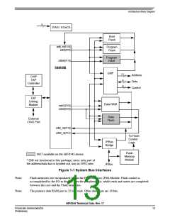
Architecture Block Diagram
5
JTAG / EOnCE
Boot
Flash
pdb_m[15:0]
pab[20:0]
Program
Flash
Program
RAM
cdbw[31:0]
56800E
EMI*
11
Address
Data
CHIP
TAP
Controller
4
6
Control
TAP
Linking
Module
Data RAM
xab1[23:0]
xab2[23:0]
Data
Flash
External
JTAG Port
cdbr_m[31:0]
xdb2_m[15:0
To Flash
Control
Logic
IPBus
Bridge
Flash
Memory
Module
NOT available on the 56F8145 device.
* EMI not functional in this package; since only part of
the address/data bus is bonded out, use as GPIO pins
IPBus
Figure 1-1 System Bus Interfaces
Note:
Note:
Flash memories are encapsulated within the Flash Memory (FM) Module. Flash control is
accomplished by the I/O to the FM over the peripheral bus, while reads and writes are completed
between the core and the Flash memories.
The primary data RAM port is 32 bits wide. Other data ports are 16 bits.
56F8345 Technical Data, Rev. 17
Freescale Semiconductor
Preliminary
13

 FREESCALE [ Freescale ]