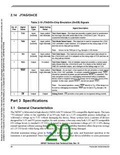
2.14 JTAG/OnCE
Table 2-19 JTAG/On-Chip Emulation (OnCE) Signals
No. of
Pins
Signal
Name
Signal
Type
State During
Reset
Signal Description
1
TCK
Input
(Schmitt)
Input, pulled Test Clock Input—This input pin provides a gated clock to synchronize
low internally the test logic and shift serial data to the JTAG/OnCE port. The pin is
connected internally to a pull-down resistor.
1
TMS
Input
(Schmitt)
Input, pulled Test Mode Select Input—This input pin is used to sequence the JTAG
high internally TAP controller’s state machine. It is sampled on the rising edge of TCK
and has an on-chip pull-up resistor.
Note: Always tie the TMS pin to VDD through a 2.2K resistor.
1
1
1
TDI
TDO
TRST
Input
(Schmitt)
Input, pulled Test Data Input—This input pin provides a serial input data stream to
high internally the JTAG/OnCE port. It is sampled on the rising edge of TCK and has an
on-chip pull-up resistor.
Output
Tri-stated
Test Data Output—This tri-statable output pin provides a serial output
data stream from the JTAG/OnCE port. It is driven in the Shift-IR and
Shift-DR controller states, and changes on the falling edge of TCK.
Input
(Schmitt)
Input, pulled Test Reset—As an input, a low signal on this pin provides a reset signal
high internally to the JTAG TAP controller. To ensure complete hardware reset, TRST
should be asserted at power-up and whenever RESET is asserted. The
only exception occurs in a debugging environment when a hardware
device reset is required and it is necessary not to reset the OnCE/JTAG
module. In this case, assert RESET, but do not assert TRST.
Note: For normal operation, connect TRST directly to VSS. If the design is to
be used in a debugging environment, TRST may be tied to VSS through a 1K
resistor.
1
DE
Output
Output
Debug Event—DE provides a low pulse on recognized debug events.
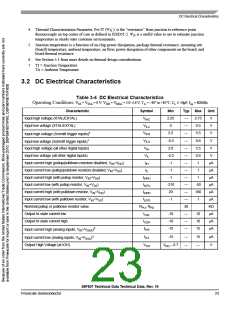
Part 3 Specifications
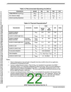
3.1 General Characteristics
The 56F807 is fabricated in high-density CMOS with 5V-tolerant TTL-compatible digital inputs. The term
“5V-tolerant” refers to the capability of an I/O pin, built on a 3.3V compatible process technology, to
withstand a voltage up to 5.5V without damaging the device. Many systems have a mixture of devices
designed for 3.3V and 5V power supplies. In such systems, a bus may carry both 3.3V and 5V-compatible
I/O voltage levels (a standard 3.3V I/O is designed to receive a maximum voltage of 3.3V ± 10% during
normal operation without causing damage). This 5V-tolerant capability therefore offers the power savings
of 3.3V I/O levels while being able to receive 5V levels without being damaged.
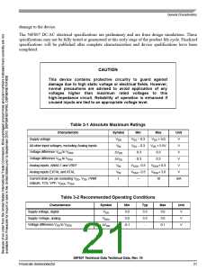
Absolute maximum ratings given in Table 3-1 are stress ratings only, and functional operation at the
maximum is not guaranteed. Stress beyond these ratings may affect device reliability or cause permanent
56F807 Technical Data Technical Data, Rev. 16
20
Freescale Semiconductor

 FREESCALE [ Freescale ]