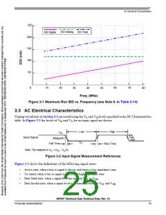
General Characteristics
damage to the device.
The 56F807 DC/AC electrical specifications are preliminary and are from design simulations. These
specifications may not be fully tested or guaranteed at this early stage of the product life cycle. Finalized
specifications will be published after complete characterization and device qualifications have been
completed.
CAUTION
This device contains protective circuitry to guard against
damage due to high static voltage or electrical fields. However,
normal precautions are advised to avoid application of any
voltages higher than maximum rated voltages to this
high-impedance circuit. Reliability of operation is enhanced if
unused inputs are tied to an appropriate voltage level.
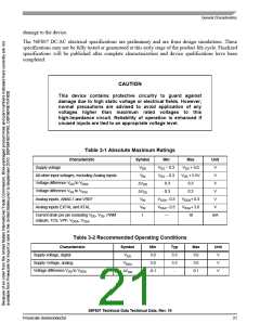
Table 3-1 Absolute Maximum Ratings
Characteristic
Symbol
VDD
VIN
Min
VSS – 0.3
VSS – 0.3
- 0.3
Max
VSS + 4.0
VSS + 5.5V
0.3
Unit
V
Supply voltage
All other input voltages, excluding Analog inputs
Voltage difference VDD to VDDA
V
ΔVDD
ΔVSS
VIN
V
Voltage difference VSS to VSSA
- 0.3
0.3
V
Analog inputs, ANA0-7 and VREF
Analog inputs EXTAL and XTAL
VSSA– 0.3
VSSA– 0.3
—
VDDA+ 0.3
VSSA+ 3.0
10
V
VIN
V
Current drain per pin excluding VDD, VSS, PWM
outputs, TCS, VPP, VDDA, VSSA
I
mA
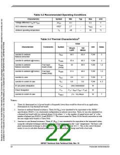
Table 3-2 Recommended Operating Conditions
Characteristic
Supply voltage, digital
Symbol
VDD
Min
3.0
Typ
3.3
3.3
-
Max
3.6
3.6
0.1
Unit
V
V
V
Supply Voltage, analog
VDDA
ΔVDD
3.0
Voltage difference VDD to VDDA
-0.1
56F807 Technical Data Technical Data, Rev. 16
Freescale Semiconductor
21

 FREESCALE [ Freescale ]