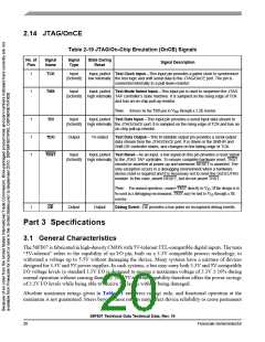
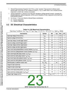
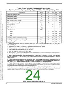
Table 3-4 DC Electrical Characteristics (Continued)
Operating Conditions: VSS = VSSA = 0 V, VDD = VDDA = 3.0–3.6 V, TA = –40° to +85°C, CL ≤ 50pF, fop = 80MHz
Characteristic
Output Low Voltage (at IOL)
Symbol
VOL
Min
—
4
Typ
—
—
—
—
—
8
Max
0.4
—
Unit
V
Output source current
Output source current
IOH
mA
mA
mA
mA
pF
IOL
4
—
PWM pin output source current3
IOHP
IOLP
CIN
10
16
—
—
—
PWM pin output sink current4
Input capacitance
—
—
Output capacitance
COUT
12
—
pF
5
V
DD supply current
Run 6
IDDT
—
—
195
170
220
200
mA
mA
Wait7
Stop
—
115
2.7
145
3.0
mA
V
Low Voltage Interrupt, external power supply8
Low Voltage Interrupt, internal power supply9
Power on Reset10
VEIO
VEIC
2.4
2.0
—
2.2
1.7
2.4
2.0
V
V
VPOR
1. Schmitt Trigger inputs are: EXTBOOT, IRQA, IRQB, RESET, TCS, ISA0-2, FAULTA0-3, ISB0-2, FAULTB0-3, TCK, TRST, TMS,
TDI, and MSCAN_RX
2. Analog inputs are: ANA[0:7], XTAL and EXTAL. Specification assumes ADC is not sampling.
3. PWM pin output source current measured with 50% duty cycle.
4. PWM pin output sink current measured with 50% duty cycle.
5. IDDT = IDD + IDDA (Total supply current for VDD + VDDA
)
6. Run (operating) IDD measured using 8MHz clock source. All inputs 0.2V from rail; outputs unloaded. All ports configured as inputs;
measured with all modules enabled.
7. Wait IDD measured using external square wave clock source (fosc = 8MHz) into XTAL; all inputs 0.2V from rail; no DC loads; less
than 50pF on all outputs. CL = 20pF on EXTAL; all ports configured as inputs; EXTAL capacitance linearly affects wait IDD; measured
with PLL enabled.
8. This low voltage interrupt monitors the VDDA external power supply. VDDA is generally connected to the same potential as VDD via
separate traces. If VDDA drops below VEIO, an interrupt is generated. Functionality of the device is guaranteed under transient condi-
tions when VDDA>VEIO (between the minimum specified VDD and the point when the VEIO interrupt is generated).
9. This low voltage interrupt monitors the internally regulated core power supply. If the output from the internal voltage is regulator
drops below VEIC, an interrupt is generated. Since the core logic supply is internally regulated, this interrupt will not be generated unless
the external power supply drops below the minimum specified value (3.0V).
10. Power–on reset occurs whenever the internally regulated 2.5V digital supply drops below 1.5V typical. While power is ramping up,
this signal remains active as long as the internal 2.5V is below 1.5V typical, no matter how long the ramp-up rate is. The internally
regulated voltage is typically 100mV less than VDD during ramp-up until 2.5V is reached, at which time it self-regulates.
56F807 Technical Data Technical Data, Rev. 16
24
Freescale Semiconductor

 FREESCALE [ Freescale ]