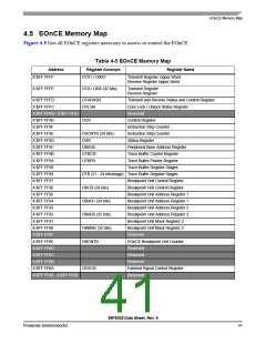
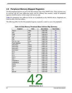
4.6 Peripheral Memory-Mapped Registers
On-chip peripheral registers are part of the data memory map on the 56800E series. These locations may
be accessed with the same addressing modes used for ordinary Data memory, except all peripheral
registers should be read or written using word accesses only.
Table 4-6 summarizes base addresses for the set of peripherals on the 56F8036 device. Peripherals are
listed in order of the base address.
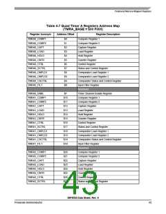
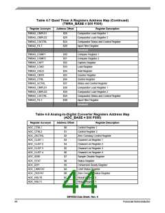
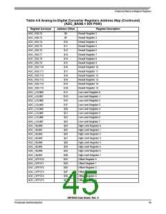
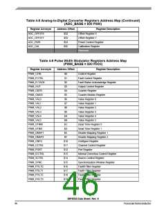
The following tables list all of the peripheral registers required to control or access the peripherals.
Table 4-6 Data Memory Peripheral Base Address Map Summary
Peripheral
Prefix
Base Address
Table Number
Timer A
ADC
TMRA
ADC
X:$00 F000
X:$00 F080
X:$00 F0C0
X:$00 F0E0
X:$00 F100
X:$00 F120
X:$00 F130
X:$00 F140
X:$00 F150
X:$00 F160
X:$00 F170
X:$00 F180
X:$00 F190
X:$00 F1A0
X:$00 F1B0
X:$00 F1C0
X:$00 F1D0
X:$00 F1E0
X:$00 F1F0
X:$00 F200
X:$00 F220
X:$00 F280
4-7
4-8
PWM
ITCN
SIM
PWM
ITCN
SIM
4-9
4-10
4-11
4-12
4-13
4-14
4-15
4-16
4-17
4-18
4-19
4-20
4-21
4-22
4-23
4-24
4-25
4-26
4-27
4-28
COP
COP
CLK, PLL, OSC
Power Supervisor
GPIO Port A
GPIO Port B
GPIO Port C
GPIO Port D
PIT 0
OCCS
PS
GPIOA
GPIOB
GPIOC
GPIOD
PIT0
PIT 1
PIT1
PIT 2
PIT2
DAC 0
DAC0
DAC1
CMPA
CMPB
SCI0
DAC 1
Comparator A
Comparator B
QSCI 0
QSPI 0
SPI0
I2C
I2C
FM
FM
X:$00 F400
X:$00 F800
4-29
4-30
MSCAN
CAN
56F8036 Data Sheet, Rev. 6
42
FreescaleSemiconductor

 FREESCALE [ Freescale ]