Program Map
1
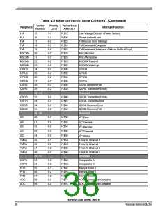
Table 4-2 Interrupt Vector Table Contents (Continued)
Vector
Number
Priority
Level
Vector Base
Address +
Peripheral
Interrupt Function
ADC
60
0-2
P:$78
P:$7A
P:$7C
P:$7E
ADC Zero Crossing or Limit Error
PWM
PWM
SWILP
61
62
63
0-2
0-2
-1
Reload PWM
PWM Fault
SW Interrupt Low Priority
1. Two words are allocated for each entry in the vector table. This does not allow the full address range to be referenced
from the vector table, providing only 19 bits of address.
2. If the VBA is set to the reset value, the first two locations of the vector table will overlay the chip reset addresses since
the reset address would match the base of this vector table.
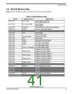
4.3 Program Map
The Program Memory map is shown in Table 4-3.
1
Table 4-3 Program Memory Map at Reset
Begin/End Address
Memory Allocation
P: $1F FFFF
RESERVED
P: $00 8800
On-Chip RAM2
8KB
P: $00 87FF
P: $00 8000
P: $00 7FFF
P: $00 0000
Internal Program Flash
64KB
Cop Reset Address = $00 0002
Boot Location = $00 0000
1. All addresses are 16-bit Word addresses.
2. This RAM is shared with Data space starting at address X: $00 0000; see Figure 4-1.
56F8036 Data Sheet, Rev. 6
Freescale Semiconductor
39

 FREESCALE [ Freescale ]