Interrupt Vector Table
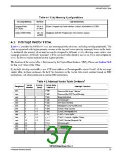
Table 4-1 Chip Memory Configurations
On-Chip Memory
56F8036
Use Restrictions
Program Flash
(PFLASH)
32k x 16
or 64KB
Erase / Program via Flash interface unit and word writes to CDBW
Usable by both the Program and Data memory spaces
Unified RAM (RAM)
4k x 16
or 8KB
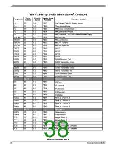
4.2 Interrupt Vector Table
Table 4-2 provides the 56F8036’s reset and interrupt priority structure, including on-chip peripherals. The
table is organized with higher-priority vectors at the top and lower-priority interrupts lower in the table.
As indicated, the priority of an interrupt can be assigned to different levels, allowing some control over
interrupt priorities. All level 3 interrupts will be serviced before level 2, and so on. For a selected priority
level, the lowest vector number has the highest priority.
The location of the vector table is determined by the Vector Base Address (VBA). Please see Section 5.6.8
for the reset value of the VBA.
By default, the chip reset address and COP reset address will correspond to vector 0 and 1 of the interrupt
vector table. In these instances, the first two locations in the vector table must contain branch or JMP
instructions. All other entries must contain JSR instructions.
1
Table 4-2 Interrupt Vector Table Contents
Vector
Number
Priority
Level
Vector Base
Address +
Peripheral
Interrupt Function
Reserved for Reset Overlay2
core
P:$00
core
core
core
core
core
core
core
core
core
core
core
core
core
P:$02
P:$04
P:$06
P:$08
P:$0A
P:$0C
P:$0E
P:$10
P:$12
P:$14
P:$16
P:$18
P:$1A
Reserved for COP Reset Overlay
Illegal Instruction
2
3
4
5
6
7
8
9
3
3
3
3
SW Interrupt 3
HW Stack Overflow
Misaligned Long Word Access
EOnCE Step Counter
EOnCE Breakpoint Unit
EOnCE Trace Buffer
EOnCE Transmit Register Empty
EOnCE Receive Register Full
SW Interrupt 2
1-3
1-3
1-3
1-3
1-3
2
10
11
12
13
14
1
SW Interrupt 1
0
SW Interrupt 0
Reserved
56F8036 Data Sheet, Rev. 6
Freescale Semiconductor
37

 FREESCALE [ Freescale ]