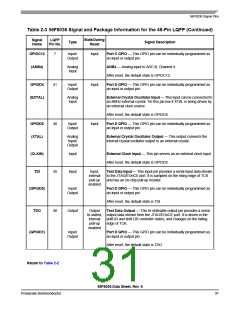
56F8036 Signal Pins
Table 2-3 56F8036 Signal and Package Information for the 48-Pin LQFP (Continued)
Signal
Name
LQFP
Pin No.
StateDuring
Reset
Type
Signal Description
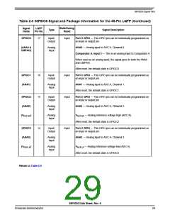
GPIOC12
(ANB4)
7
Input/
Output
Input
Port C GPIO — This GPIO pin can be individually programmed as
an input or output pin.
Analog
Input
ANB4 — Analog input to ADC B, Channel 4.
After reset, the default state is GPIOC12.
GPIOD4
(EXTAL)
41
Input/
Output
Input
Port D GPIO — This GPIO pin can be individually programmed as
an input or output pin.
Analog
Input
External Crystal Oscillator Input — This input can be connected to
an 8MHz external crystal. Tie this pin low if XTAL is being driven by
an external clock source.
After reset, the default state is GPIOD4.
GPIOD5
(XTAL)
40
Input/
Output
Input
Port D GPIO — This GPIO pin can be individually programmed as
an input or output pin.
Analog
Input/
External Crystal Oscillator Output — This output connects the
internal crystal oscillator output to an external crystal.
Output
(CLKIN)
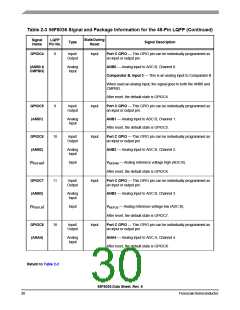
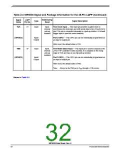
TDI
Input
External Clock Input — This pin serves as an external clock input.
After reset, the default state is GPIOD5.
45
Input
Input,
internal
pull-up
enabled
Test Data Input — This input pin provides a serial input data stream
to the JTAG/EOnCE port. It is sampled on the rising edge of TCK
and has an on-chip pull-up resistor.
(GPIOD0)
Input/
Port D GPIO — This GPIO pin can be individually programmed as
Output
an input or output pin.
After reset, the default state is TDI.
TDO
48
Output
Output
Test Data Output — This tri-stateable output pin provides a serial
tri-stated, output data stream from the JTAG/EOnCE port. It is driven in the
internal
pull-up
shift-IR and shift-DR controller states, and changes on the falling
edge of TCK.
enabled
(GPIOD1)
Input/
Port D GPIO — This GPIO pin can be individually programmed as
Output
an input or output pin.
After reset, the default state is TDO.
Return to Table 2-2
56F8036 Data Sheet, Rev. 6
Freescale Semiconductor
31

 FREESCALE [ Freescale ]